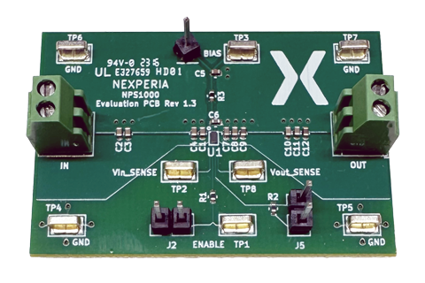
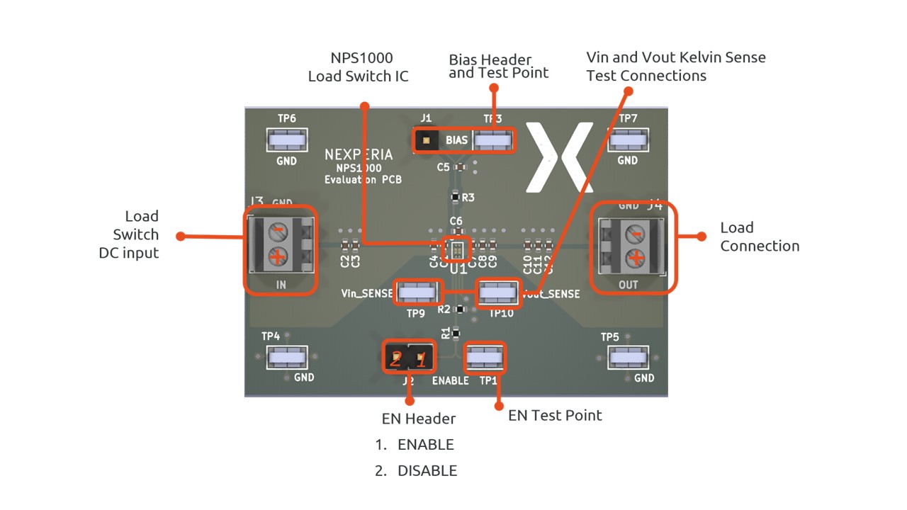
NEVB-NPS1000 load switch evaluation board
The NEVB-NPS1000 is a two-layer PCB containing the NPS1000 load switch device. The VIN and
VOUT connections to the device and the PCB layout routing provides a low-resistance pathway into and
out of the device under test. Test point connections allow the EVB user to control the device with userdefined test conditions and make accurate device measurements.
Key features and benefits
• Input operating voltage range (VIN): 0.5 V to 1 V
• Rated currents: 0.6A RMS, 1.5A peak
• ON resistance (RDS(on)): 11 mΩ (typical) at 25C
• Controlled Startup
• <200us from enable to full enhancement of power FET
• Output short tolerant
• When supplied by a 4.5A current limited power supply
• Over-Temperature Shutdown and Input UVLO Protection
• 8Ω Discharge While Disabled
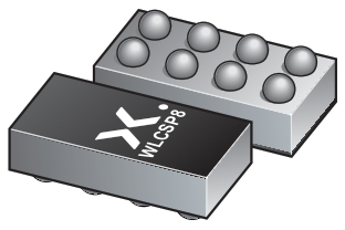
• WLCSP package footprint
• Convenient connections via test points and INPUT/OUTPUT terminals
Products on the board (1)
| Type number | Description | Status | Quick access | |
|---|---|---|---|---|
|
NPS1000UP | 0.5 V to 1.0 V, 1.5 A peak, 11 mΩ, load switch | Production |
Products on the board (1)
| Type number | Description | Status | Quick access | |
|---|---|---|---|---|
|
|
NPS1000UP | 0.5 V to 1.0 V, 1.5 A peak, 11 mΩ, load switch | Production |
Documentation (2)
Support
If you are in need of design/technical support, let us know and fill in the answer form, we'll get back to you shortly.