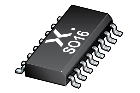
Orderable parts
| Type number | Orderable part number | Ordering code (12NC) | Package | Buy from distributors |
|---|---|---|---|---|
| 74HC191D | 74HC191D,653 | 933714600653 | SOT109-1 | Order product |
Discover Nexperia’s extensive portfolio of diodes, bipolar transistors, ESD protection devices, MOSFETs, GaN FETs, IGBTs, and analog & logic ICs. Our components power virtually every electronic design worldwide - from automotive and industrial to mobile and consumer applications.
Our products find applications across various industries, from automotive and industrial to power, computing, consumer, mobile, and wearables. With a commitment to innovation and sustainability, our components set benchmarks in efficiency, empowering our global customer base to develop energy-efficient and cutting-edge solutions.
Try out our devices and their performance with our comprehensive range of evaluation boards. Gain a deeper understanding of how our products can benefit your application, whether it's optimizing for efficiency, robustness, or reliability. You can find Application focus, Package focus, and different Nexperia Product focus boards here.

Register once, drag and drop ECAD models into your CAD tool and speed up your design.
Click here for more informationPresettable synchronous 4-bit binary up/down counter
The 74HC191 is an asynchronously presettable 4-bit binary up/down counter. It contains four master/slave flip-flops with internal gating and steering logic to provide asynchronous preset and synchronous count-up and count-down operation. Asynchronous parallel load capability permits the counter to be preset to any desired value. Information present on the parallel data inputs (D0 to D3) is loaded into the counter and appears on the outputs when the parallel load (PL) input is LOW. This operation overrides the counting function. Counting is inhibited by a HIGH level on the count enable (CE) input. When CE is LOW internal state changes are initiated synchronously by the LOW-to-HIGH transition of the clock input. The up/down (U/D) input signal determines the direction of counting as indicated in the function table. The CE input may go LOW when the clock is in either state, however, the LOW-to-HIGH CE transition must occur only when the clock is HIGH. Also, the U/D input should be changed only when either CE or CP is HIGH. Overflow/underflow indications are provided by two types of outputs, the terminal count (TC) and ripple clock (RC). The TC output is normally LOW and goes HIGH when a circuit reaches zero in the count-down mode or reaches '15' in the count-up-mode. The TC output will remain HIGH until a state change occurs, either by counting or presetting, or until U/D is changed. Do not use the TC output as a clock signal because it is subject to decoding spikes. The TC signal is used internally to enable the RC output. When TC is HIGH and CE is LOW, the RC output follows the clock pulse (CP). This feature simplifies the design of multistage counters as shown in Figure 1 and Figure 2. In Figure 1, each RC output is used as the clock input to the next higher stage. It is only necessary to inhibit the first stage to prevent counting in all stages, since a HIGH on CE inhibits the RC output pulse. The timing skew between state changes in the first and last stages is represented by the cumulative delay of the clock as it ripples through the preceding stages. This can be a disadvantage of this configuration in some applications. Figure 2 shows a method of causing state changes to occur simultaneously in all stages. The RC outputs propagate the carry/borrow signals in ripple fashion and all clock inputs are driven in parallel. In this configuration the duration of the clock LOW state must be long enough to allow the negative-going edge of the carry/borrow signal to ripple through to the last stage before the clock goes HIGH. Since the RC output of any package goes HIGH shortly after its CP input goes HIGH there is no such restriction on the HIGH-state duration of the clock. In Figure 3, the configuration shown avoids ripple delays and their associated restrictions. Combining the TC signals from all the preceding stages forms the CE input for a given stage. An enable must be included in each carry gate in order to inhibit counting. The TC output of a given stage it not affected by its own CE signal therefore the simple inhibit scheme of Figure 1 and Figure 2 does not apply. Inputs include clamp diodes. This enables the use of current limiting resistors to interface inputs to voltages in excess of VCC.
Wide supply voltage range from 2.0 to 6.0 V
CMOS low power dissipation
High noise immunity
Latch-up performance exceeds 100 mA per JESD 78 Class II Level B
CMOS input levels
Synchronous reversible counting
Asynchronous parallel load
Count enable control for synchronous expansion
Single up/down control input
Complies with JEDEC standards:
JESD8C (2.7 V to 3.6 V)
JESD7A (2.0 V to 6.0 V)
ESD protection:
HBM: ANSI/ESDA/JEDEC JS-001 class 2 exceeds 2000 V
CDM: ANSI/ESDA/JEDEC JS-002 class C3 exceeds 1000 V
Specified from -40 °C to +85 °C and -40 °C to +125 °C
| Type number | VCC (V) | Output drive capability (mA) | Logic switching levels | tpd (ns) | Power dissipation considerations | Tamb (°C) | Rth(j-a) (K/W) | Ψth(j-top) (K/W) | Rth(j-c) (K/W) | Package name |
|---|---|---|---|---|---|---|---|---|---|---|
| 74HC191D | 2.0 - 6.0 | ± 5.2 | CMOS | 22 | low | -40~125 | 67 | 1 | 24 | SO16 |
| Type number | Orderable part number, (Ordering code (12NC)) | Status | Marking | Package | Package information | Reflow-/Wave soldering | Packing |
|---|---|---|---|---|---|---|---|
| 74HC191D | 74HC191D,653 (933714600653) |
Active | 74HC191D |

SO16 (SOT109-1) |
SOT109-1 |
SO-SOJ-REFLOW
SO-SOJ-WAVE WAVE_BG-BD-1 |
Not available |
| Type number | Orderable part number | Chemical content | RoHS | RHF-indicator |
|---|---|---|---|---|
| 74HC191D | 74HC191D,653 | 74HC191D |
|
|
| File name | Title | Type | Date |
|---|---|---|---|
| 74HC191 | Presettable synchronous 4-bit binary up/down counter | Data sheet | 2024-03-14 |
| AN11044 | Pin FMEA 74HC/74HCT family | Application note | 2019-01-09 |
| AN90063 | Questions about package outline drawings | Application note | 2025-03-12 |
| SOT109-1 | 3D model for products with SOT109-1 package | Design support | 2020-01-22 |
| Nexperia_package_poster | Nexperia package poster | Leaflet | 2020-05-15 |
| SO16_SOT109-1_mk | plastic, small outline package; 16 leads; 1.27 mm pitch; 9.9 mm x 3.9 mm x 1.35 mm body | Marcom graphics | 2017-01-28 |
| SOT109-1 | plastic, small outline package; 16 leads; 1.27 mm pitch; 9.9 mm x 3.9 mm x 1.75 mm body | Package information | 2023-11-07 |
| 74HC191D_Nexperia_Product_Reliability | 74HC191D Nexperia Product Reliability | Quality document | 2025-03-20 |
| SO-SOJ-REFLOW | Footprint for reflow soldering | Reflow soldering | 2009-10-08 |
| HCT_USER_GUIDE | HC/T User Guide | User manual | 1997-10-31 |
| SO-SOJ-WAVE | Footprint for wave soldering | Wave soldering | 2009-10-08 |
| WAVE_BG-BD-1 | Wave soldering profile | Wave soldering | 2021-09-08 |
If you are in need of design/technical support, let us know and fill in the answer form we'll get back to you shortly.
The Nexperia Longevity Program is aimed to provide our customers information from time to time about the expected time that our products can be ordered. The NLP is reviewed and updated regularly by our Executive Management Team. View our longevity program here.
| File name | Title | Type | Date |
|---|---|---|---|
| SOT109-1 | 3D model for products with SOT109-1 package | Design support | 2020-01-22 |
| Type number | Orderable part number | Ordering code (12NC) | Status | Packing | Packing Quantity | Buy online |
|---|---|---|---|---|---|---|
| 74HC191D | 74HC191D,653 | 933714600653 | Active | Not available | 2,500 |
|
As a Nexperia customer you can order samples via our sales organization.
If you do not have a direct account with Nexperia our network of global and regional distributors is available and equipped to support you with Nexperia samples. Check out the list of official distributors.
The interactive datasheets are based on the Nexperia MOSFET precision electrothermal models. With our interactive datasheets you can simply specify your own conditions interactively. Start by changing the values of the conditions. You can do this by using the sliders in the condition fields. By dragging the sliders you will see how the MOSFET will perform at the new conditions set.