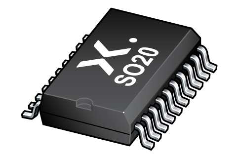
Register once, drag and drop ECAD models into your CAD tool and speed up your design.
Click here for more information74HC299DB
8-bit universal shift register; 3-state
The 74HC299 is an 8-bit universal shift register with 3-state outputs. It contains eight edge-triggered D-type flip-flops and the interstage logic necessary to perform synchronous shift-right, shift-left, parallel load and hold operations. The type of operation is determined by the mode select inputs S0 and S1. Pins I/O0 to I/O7 are flip-flop 3-state buffer outputs which allow them to operate as data inputs in parallel load mode. The serial outputs Q0 and Q7 are used for expansion in serial shifting of longer words. A LOW signal on the asynchronous master reset input MR overrides the Sn and clock CP inputs and resets the flip-flops. All other state changes are initiated by the rising edge of the clock pulse. Inputs can change when the clock is either state, provided that the recommended set-up and hold times are observed. A HIGH signal on the 3-state output enable inputs OE1 or OE2 disables the 3-state buffers and the I/On outputs assume a high-impedance OFF-state. In this condition, the shift, hold, load and reset operations can still occur. The 3-state buffers are also disabled by HIGH signals on both S0 and S1, when in preparation for a parallel load operation. Inputs include clamp diodes. This enables the use of current limiting resistors to interface inputs to voltages in excess of VCC.
Alternatives
Features and benefits
CMOS input levels
Multiplexed inputs/outputs provide improved bit density
Four operating modes:
Shift left
Shift right
Hold (store)
Load data
Operates with output enable or at high-impedance OFF-state
3-state outputs drive bus lines directly
Cascadable for n-bit word lengths
ESD protection:
HBM: ANSI/ESDA/JEDEC JS-001 class 2 exceeds 2000 V
CDM: ANSI/ESDA/JEDEC JS-002 class C3 exceeds 1000 V
Specified from -40 °C to +85 °C and from -40 °C to +125 °C
PCB Symbol, Footprint and 3D Model
| Model Name | Description |
|---|---|
|
|
Package
All type numbers in the table below are discontinued.
| Type number | Orderable part number, (Ordering code (12NC)) | Status | Marking | Package | Package information | Reflow-/Wave soldering | Packing |
|---|---|---|---|---|---|---|---|
| 74HC299DB | 74HC299DB,112 (935189890112) |
Obsolete | no package information | ||||
| 74HC299DB,118 (935189890118) |
Obsolete | ||||||
Environmental information
All type numbers in the table below are discontinued.
| Type number | Orderable part number | Chemical content | RoHS | RHF-indicator |
|---|---|---|---|---|
| 74HC299DB | 74HC299DB,112 | 74HC299DB |
|
|
| 74HC299DB | 74HC299DB,118 | 74HC299DB |
|
|
Documentation (2)
| File name | Title | Type | Date |
|---|---|---|---|
| AN11044 | Pin FMEA 74HC/74HCT family | Application note | 2019-01-09 |
| HCT_USER_GUIDE | HC/T User Guide | User manual | 1997-10-31 |
Support
If you are in need of design/technical support, let us know and fill in the answer form we'll get back to you shortly.
Longevity
The Nexperia Longevity Program is aimed to provide our customers information from time to time about the expected time that our products can be ordered. The NLP is reviewed and updated regularly by our Executive Management Team. View our longevity program here.
Models
No documents available
PCB Symbol, Footprint and 3D Model
| Model Name | Description |
|---|---|
|
|
How does it work?
The interactive datasheets are based on the Nexperia MOSFET precision electrothermal models. With our interactive datasheets you can simply specify your own conditions interactively. Start by changing the values of the conditions. You can do this by using the sliders in the condition fields. By dragging the sliders you will see how the MOSFET will perform at the new conditions set.
