Register once, drag and drop ECAD models into your CAD tool and speed up your design.
Click here for more information74HCT30DB
8-input NAND gate
The 74HC30; 74HCT30 is an 8-input NAND gate. Inputs include clamp diodes. This enables the use of current limiting resistors to interface inputs to voltages in excess of VCC.
Alternatives
Features and benefits
Wide supply voltage range from 2.0 V to 6.0 V
CMOS low power dissipation
High noise immunity
Latch-up performance exceeds 100 mA per JESD 78 Class II Level B
Complies with JEDEC standards:
- JESD8C (2.7 V to 3.6 V)
- JESD7A (2.0 V to 6.0 V)
Input levels:
For 74HC30: CMOS level
For 74HCT30: TTL level
ESD protection:
HBM: ANSI/ESDA/JEDEC JS-001 class 2 exceeds 2000 V
CDM: ANSI/ESDA/JEDEC JS-002 class C3 exceeds 1000 V
Specified from -40 °C to +85 °C and from -40 °C to +125 °C
Parametrics
| Type number | Package name |
|---|---|
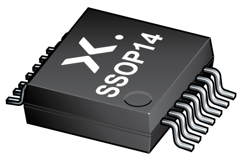
| 74HCT30DB | SSOP14 |
PCB Symbol, Footprint and 3D Model
| Model Name | Description |
|---|---|
|
Register once, drag and drop ECAD models into your CAD tool and speed up your design. Click here for more information |
Package
All type numbers in the table below are discontinued.
| Type number | Orderable part number, (Ordering code (12NC)) | Status | Marking | Package | Package information | Reflow-/Wave soldering | Packing |
|---|---|---|---|---|---|---|---|
| 74HCT30DB | 74HCT30DB,112 (935189310112) |
Obsolete | HCT30 |

SSOP14 (SOT337-1) |
SOT337-1 |
SSOP-TSSOP-VSO-REFLOW
SSOP-TSSOP-VSO-WAVE |
Not available |
| 74HCT30DB,118 (935189310118) |
Obsolete | HCT30 | SOT337-1_118 |
Environmental information
All type numbers in the table below are discontinued.
| Type number | Orderable part number | Chemical content | RoHS | RHF-indicator |
|---|---|---|---|---|
| 74HCT30DB | 74HCT30DB,112 | 74HCT30DB |
|
|
| 74HCT30DB | 74HCT30DB,118 | 74HCT30DB |
|
|
Series
Documentation (8)
| File name | Title | Type | Date |
|---|---|---|---|
| 74HC_HCT30 | 8-input NAND gate | Data sheet | 2024-03-13 |
| AN11044 | Pin FMEA 74HC/74HCT family | Application note | 2019-01-09 |
| Nexperia_package_poster | Nexperia package poster | Leaflet | 2020-05-15 |
| SSOP14_SOT337-1_mk | plastic, shrink small outline package; 14 leads; 0.65 mm pitch; 6.2 mm x 5.3 mm x 2 mm body | Marcom graphics | 2017-01-28 |
| SOT337-1 | plastic, shrink small outline package; 14 leads; 0.65 mm pitch; 6.2 mm x 5.3 mm x 2 mm body | Package information | 2020-04-21 |
| SSOP-TSSOP-VSO-REFLOW | Footprint for reflow soldering | Reflow soldering | 2009-10-08 |
| HCT_USER_GUIDE | HC/T User Guide | User manual | 1997-10-31 |
| SSOP-TSSOP-VSO-WAVE | Footprint for wave soldering | Wave soldering | 2009-10-08 |
Support
If you are in need of design/technical support, let us know and fill in the answer form we'll get back to you shortly.
Longevity
The Nexperia Longevity Program is aimed to provide our customers information from time to time about the expected time that our products can be ordered. The NLP is reviewed and updated regularly by our Executive Management Team. View our longevity program here.
Models
No documents available
PCB Symbol, Footprint and 3D Model
| Model Name | Description |
|---|---|
|
Register once, drag and drop ECAD models into your CAD tool and speed up your design. Click here for more information |
How does it work?
The interactive datasheets are based on the Nexperia MOSFET precision electrothermal models. With our interactive datasheets you can simply specify your own conditions interactively. Start by changing the values of the conditions. You can do this by using the sliders in the condition fields. By dragging the sliders you will see how the MOSFET will perform at the new conditions set.
