
74ALVCH16821
Parametrics
| Type number | VCC (V) | Logic switching levels | Output drive capability (mA) | tpd (ns) | fmax (MHz) | Power dissipation considerations | Tamb (°C) | Rth(j-a) (K/W) | Ψth(j-top) (K/W) | Package name |
|---|---|---|---|---|---|---|---|---|---|---|
| 74ALVCH16821DGG | 1.2 - 3.6 | TTL | ± 24 | 2.5 | 350 | low | -40~85 | 93 | 21 | TSSOP56 |
Package
| Type number | Orderable part number, (Ordering code (12NC)) | Status | Marking | Package | Package information | Reflow-/Wave soldering | Packing |
|---|---|---|---|---|---|---|---|
| 74ALVCH16821DGG | 74ALVCH16821DGG,11 (935259010118) |
Active | ALVCH16821 |
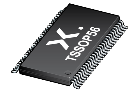
TSSOP56 (SOT364-1) |
SOT364-1 |
SSOP-TSSOP-VSO-WAVE
|
SOT364-1_118 |
All type numbers in the table below are discontinued.
| Type number | Orderable part number, (Ordering code (12NC)) | Status | Marking | Package | Package information | Reflow-/Wave soldering | Packing |
|---|---|---|---|---|---|---|---|
| 74ALVCH16821DL | 74ALVCH16821DL,512 (935259000512) |
Obsolete | ALVCH16821 Standard Procedure Standard Procedure |
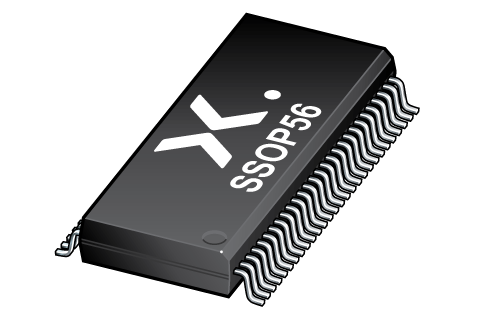
SSOP56 (SOT371-1) |
SOT371-1 |
SSOP-TSSOP-VSO-REFLOW
SSOP-TSSOP-VSO-WAVE |
Not available |
| 74ALVCH16821DL,518 (935259000518) |
Obsolete | ALVCH16821 Standard Procedure Standard Procedure | Not available | ||||
| 74ALVCH16821DL,112 (935259000112) |
Obsolete | ALVCH16821 Standard Procedure Standard Procedure | Not available | ||||
| 74ALVCH16821DL,118 (935259000118) |
Obsolete | ALVCH16821 Standard Procedure Standard Procedure | Not available |
Environmental information
| Type number | Orderable part number | Chemical content | RoHS | RHF-indicator |
|---|---|---|---|---|
| 74ALVCH16821DGG | 74ALVCH16821DGG,11 | 74ALVCH16821DGG |
|
|
All type numbers in the table below are discontinued.
| Type number | Orderable part number | Chemical content | RoHS | RHF-indicator |
|---|---|---|---|---|
| 74ALVCH16821DL | 74ALVCH16821DL,512 | 74ALVCH16821DL |
|
|
| 74ALVCH16821DL | 74ALVCH16821DL,518 | 74ALVCH16821DL |
|
|
| 74ALVCH16821DL | 74ALVCH16821DL,112 | 74ALVCH16821DL |
|
|
| 74ALVCH16821DL | 74ALVCH16821DL,118 | 74ALVCH16821DL |
|
|
Documentation (11)
| File name | Title | Type | Date |
|---|---|---|---|
| 74ALVCH16821 | 20-bit bus-interface D-type flip-flop; positive-edge trigger; 3-state | Data sheet | 2024-07-09 |
| AN90063 | Questions about package outline drawings | Application note | 2025-03-12 |
| sh00004 | Block diagram: 74ABT16821ADGG, 74ABT16821ADL, 74ALVCH16821DGG, 74ALVCH16821DL, 74ALVT162821DGG, 74ALVT162821DL | Block diagram | 2009-11-04 |
| SOT364-1 | 3D model for products with SOT364-1 package | Design support | 2020-01-22 |
| alvch16821 | alvch16821 IBIS model | IBIS model | 2013-04-08 |
| Nexperia_package_poster | Nexperia package poster | Leaflet | 2020-05-15 |
| SOT364-1 | plastic, thin shrink small outline package; 56 leads; 0.5 mm pitch; 14 mm x 6.1 mm x 1.2 mm body | Package information | 2022-06-23 |
| SOT371-1 | plastic, shrink small outline package; 56 leads; 0.635 mm pitch; 18.45 mm x 7.5 mm x 2.8 mm body | Package information | 2020-04-21 |
| SSOP-TSSOP-VSO-REFLOW | Footprint for reflow soldering | Reflow soldering | 2009-10-08 |
| Nexperia_Selection_guide_2023 | Nexperia Selection Guide 2023 | Selection guide | 2023-05-10 |
| SSOP-TSSOP-VSO-WAVE | Footprint for wave soldering | Wave soldering | 2009-10-08 |
Support
If you are in need of design/technical support, let us know and fill in the answer form we'll get back to you shortly.
Models
| File name | Title | Type | Date |
|---|---|---|---|
| SOT364-1 | 3D model for products with SOT364-1 package | Design support | 2020-01-22 |
| alvch16821 | alvch16821 IBIS model | IBIS model | 2013-04-08 |
Ordering, pricing & availability
Sample
As a Nexperia customer you can order samples via our sales organization.
If you do not have a direct account with Nexperia our network of global and regional distributors is available and equipped to support you with Nexperia samples. Check out the list of official distributors.