
74LVC2G66
Parametrics
| Type number | Configuration | VCC (V) | Logic switching levels | RON (Ω) | RON(FLAT) (Ω) | f(-3dB) (MHz) | THD (%) | Xtalk (dB) | Power dissipation considerations | Tamb (°C) | Rth(j-a) (K/W) | Ψth(j-top) (K/W) | Rth(j-c) (K/W) | Package name |
|---|---|---|---|---|---|---|---|---|---|---|---|---|---|---|
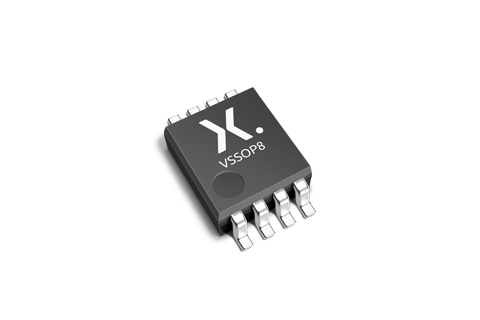
| 74LVC2G66DC | SPST-NO | 1.65 - 5.5 | CMOS/LVTTL | 15 | 1.5 | 440 | 0.005 | - | very low | -40~125 | 192 | 26.5 | 101 | VSSOP8 |
| 74LVC2G66DP | SPST-NO | 2.3 - 5.5 | CMOS/LVTTL | 15 | 1.5 | 440 | 0.005 | - | very low | -40~125 | 196 | 15.1 | 99 | TSSOP8 |
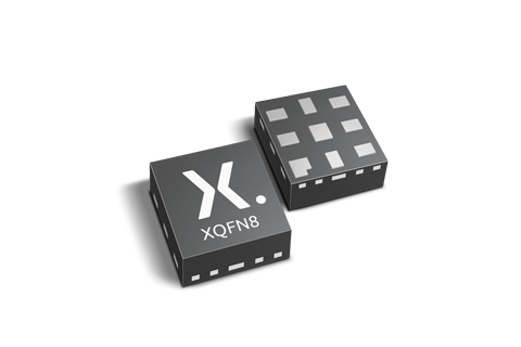
| 74LVC2G66GN | SPST-NO | 2.3 - 5.5 | CMOS/LVTTL | 15 | 1.5 | 440 | 0.005 | - | very low | -40~125 | 209 | 5.7 | 125 | XSON8 |
| 74LVC2G66GT | SPST-NO | 2.3 - 5.5 | CMOS/LVTTL | 15 | 1.5 | 440 | 0.005 | - | very low | -40~125 | 285 | 3.8 | 128 | XSON8 |
Package
| Type number | Orderable part number, (Ordering code (12NC)) | Status | Marking | Package | Package information | Reflow-/Wave soldering | Packing |
|---|---|---|---|---|---|---|---|
| 74LVC2G66DC | 74LVC2G66DC,125 (935274429125) |
Active | V66 |
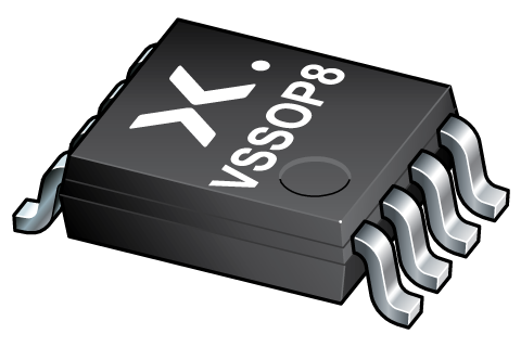
VSSOP8 (SOT765-1) |
SOT765-1 | SOT765-1_125 | |
| 74LVC2G66DP | 74LVC2G66DP,125 (935274428125) |
Active | V66 |
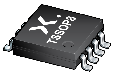
TSSOP8 (SOT505-2) |
SOT505-2 | SOT505-2_125 | |
| 74LVC2G66GN | 74LVC2G66GN,115 (935292247115) |
Active | VL |
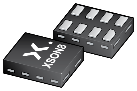
XSON8 (SOT1116) |
SOT1116 |
REFLOW_BG-BD-1
|
SOT1116_115 |
| 74LVC2G66GT | 74LVC2G66GT,115 (935280087115) |
Active | V66 |
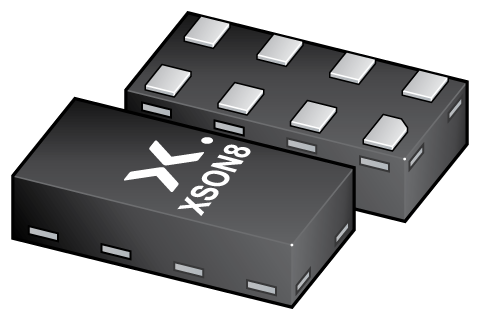
XSON8 (SOT833-1) |
SOT833-1 | SOT833-1_115 |
All type numbers in the table below are discontinued.
| Type number | Orderable part number, (Ordering code (12NC)) | Status | Marking | Package | Package information | Reflow-/Wave soldering | Packing |
|---|---|---|---|---|---|---|---|
| 74LVC2G66GM | 74LVC2G66GM,125 (935280572125) |
Obsolete |
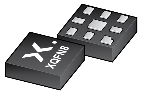
XQFN8 (SOT902-2) |
SOT902-2 | SOT902-2_125 |
Environmental information
| Type number | Orderable part number | Chemical content | RoHS | RHF-indicator |
|---|---|---|---|---|
| 74LVC2G66DC | 74LVC2G66DC,125 | 74LVC2G66DC |
|
|
| 74LVC2G66DP | 74LVC2G66DP,125 | 74LVC2G66DP |
|
|
| 74LVC2G66GN | 74LVC2G66GN,115 | 74LVC2G66GN |
|
|
| 74LVC2G66GT | 74LVC2G66GT,115 | 74LVC2G66GT |
|
|
All type numbers in the table below are discontinued.
| Type number | Orderable part number | Chemical content | RoHS | RHF-indicator |
|---|---|---|---|---|
| 74LVC2G66GM | 74LVC2G66GM,125 | 74LVC2G66GM |
|
|
Documentation (25)
| File name | Title | Type | Date |
|---|---|---|---|
| 74LVC2G66 | Bilateral switch | Data sheet | 2023-08-23 |
| AN10161 | PicoGate Logic footprints | Application note | 2002-10-29 |
| AN11009 | Pin FMEA for LVC family | Application note | 2019-01-09 |
| AN90063 | Questions about package outline drawings | Application note | 2025-03-12 |
| 001aaa532 | Block diagram: 74LVC2G66DC, 74LVC2G66DP, 74LVC2G66GM, 74LVC2G66GT, 74LVCV2G66DC, 74LVCV2G66DP | Block diagram | 2009-11-04 |
| Nexperia_document_guide_MiniLogic_PicoGate_201901 | PicoGate leaded logic portfolio guide | Brochure | 2019-01-07 |
| Nexperia_document_guide_MiniLogic_MicroPak_201808 | MicroPak leadless logic portfolio guide | Brochure | 2018-09-03 |
| SOT765-1 | 3D model for products with SOT765-1 package | Design support | 2020-01-22 |
| SOT505-2 | 3D model for products with SOT505-2 package | Design support | 2019-01-18 |
| SOT1116 | 3D model for products with SOT1116 package | Design support | 2023-02-02 |
| SOT833-1 | 3D model for products with SOT833-1 package | Design support | 2021-01-28 |
| lvc2g66 | 74LVC2G66 IBIS model | IBIS model | 2015-02-19 |
| Nexperia_package_poster | Nexperia package poster | Leaflet | 2020-05-15 |
| VSSOP8_SOT765-1_mk | plastic, very thin shrink small outline package; 8 leads; 0.5 mm pitch; 2 mm x 2.3 mm x 1 mm body | Marcom graphics | 2017-01-28 |
| XQFN8_SOT902-2_mk | plastic, extremely thin quad flat package; 8 terminals; 0.55 mm pitch; 1.6 mm x 1.6 mm x 0.5 mm body | Marcom graphics | 2017-01-28 |
| SOT765-1 | plastic, very thin shrink small outline package; 8 leads; 0.5 mm pitch; 2 mm x 2.3 mm x 1 mm body | Package information | 2022-06-03 |
| SOT505-2 | plastic, thin shrink small outline package; 8 leads; 0.65 mm pitch; 3 mm x 3 mm x 1.1 mm body | Package information | 2022-06-03 |
| SOT996-2 | plastic, leadless extremely thin small outline package; 8 terminals; 0.5 mm pitch; 3 mm x 2 mm x 0.5 mm body | Package information | 2020-04-21 |
| SOT902-2 | plastic, leadless extremely thin quad flat package; 8 terminals; 0.5 mm pitch; 1.6 mm x 1.6 mm x 0.5 mm body | Package information | 2020-04-21 |
| SOT1116 | plastic, leadless extremely thin small outline package; 8 terminals; 0.3 mm pitch; 1.2 mm x 1 mm x 0.35 mm body | Package information | 2022-06-02 |
| SOT833-1 | plastic, leadless extremely thin small outline package; 8 terminals; 0.5 mm pitch; 1 mm x 1.95 mm x 0.5 mm body | Package information | 2022-06-03 |
| REFLOW_BG-BD-1 | Reflow soldering profile | Reflow soldering | 2021-04-06 |
| Nexperia_Selection_guide_2023 | Nexperia Selection Guide 2023 | Selection guide | 2023-05-10 |
| MAR_SOT1116 | MAR_SOT1116 Topmark | Top marking | 2013-06-03 |
| MAR_SOT833 | MAR_SOT833 Topmark | Top marking | 2013-06-03 |
Support
If you are in need of design/technical support, let us know and fill in the answer form we'll get back to you shortly.
Models
| File name | Title | Type | Date |
|---|---|---|---|
| SOT765-1 | 3D model for products with SOT765-1 package | Design support | 2020-01-22 |
| SOT505-2 | 3D model for products with SOT505-2 package | Design support | 2019-01-18 |
| SOT1116 | 3D model for products with SOT1116 package | Design support | 2023-02-02 |
| SOT833-1 | 3D model for products with SOT833-1 package | Design support | 2021-01-28 |
| lvc2g66 | 74LVC2G66 IBIS model | IBIS model | 2015-02-19 |
Ordering, pricing & availability
Sample
As a Nexperia customer you can order samples via our sales organization.
If you do not have a direct account with Nexperia our network of global and regional distributors is available and equipped to support you with Nexperia samples. Check out the list of official distributors.