74AVCH1T45-Q100
Parametrics
| Type number | VCC(A) (V) | VCC(B) (V) | Logic switching levels | Output drive capability (mA) | tpd (ns) | Nr of bits | Power dissipation considerations | Tamb (°C) | Rth(j-a) (K/W) | Ψth(j-top) (K/W) | Rth(j-c) (K/W) | Package name |
|---|---|---|---|---|---|---|---|---|---|---|---|---|
| 74AVCH1T45GW-Q100 | 0.8 - 3.6 | 0.8 - 3.6 | CMOS/LVTTL | ± 12 | 2.1 | 1 | very low | -40~125 | 262 | 36.1 | 150 | TSSOP6 |
Package
| Type number | Orderable part number, (Ordering code (12NC)) | Status | Marking | Package | Package information | Reflow-/Wave soldering | Packing |
|---|---|---|---|---|---|---|---|
| 74AVCH1T45GW-Q100 | 74AVCH1T45GW-Q100H (935299267125) |
Active | K5 |
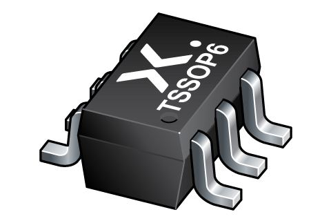
TSSOP6 (SOT363-2) |
SOT363-2 | SOT363-2_125 |
Environmental information
| Type number | Orderable part number | Chemical content | RoHS | RHF-indicator |
|---|---|---|---|---|
| 74AVCH1T45GW-Q100 | 74AVCH1T45GW-Q100H | 74AVCH1T45GW-Q100 |
|
|
Documentation (7)
| File name | Title | Type | Date |
|---|---|---|---|
| 74AVCH1T45_Q100 | Dual-supply voltage level translator/transceiver; 3-state | Data sheet | 2024-07-02 |
| AN10161 | PicoGate Logic footprints | Application note | 2002-10-29 |
| AN90007 | Pin FMEA for AVC family | Application note | 2018-11-30 |
| SOT363-2 | 3D model for products with SOT363-2 package | Design support | 2023-02-02 |
| avch1t45 | 74AVCH1T45 Ibis model | IBIS model | 2014-10-14 |
| SOT363-2 | plastic thin shrink small outline package; 6 leads; body width 1.25 mm | Package information | 2022-11-21 |
| Nexperia_Selection_guide_2023 | Nexperia Selection Guide 2023 | Selection guide | 2023-05-10 |
Support
If you are in need of design/technical support, let us know and fill in the answer form we'll get back to you shortly.
Ordering, pricing & availability
Sample
As a Nexperia customer you can order samples via our sales organization.
If you do not have a direct account with Nexperia our network of global and regional distributors is available and equipped to support you with Nexperia samples. Check out the list of official distributors.