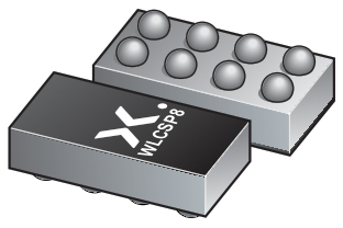
Orderable parts
| Type number | Orderable part number | Ordering code (12NC) | Package | Buy from distributors |
|---|---|---|---|---|
| NPS1001UP | NPS1001UPZ | 935692138336 | WLCSP8_SOT8068 | Order product |
Discover Nexperia’s extensive portfolio of diodes, bipolar transistors, ESD protection devices, MOSFETs, GaN FETs, IGBTs, and analog & logic ICs. Our components power virtually every electronic design worldwide - from automotive and industrial to mobile and consumer applications.
Our products find applications across various industries, from automotive and industrial to power, computing, consumer, mobile, and wearables. With a commitment to innovation and sustainability, our components set benchmarks in efficiency, empowering our global customer base to develop energy-efficient and cutting-edge solutions.
Try out our devices and their performance with our comprehensive range of evaluation boards. Gain a deeper understanding of how our products can benefit your application, whether it's optimizing for efficiency, robustness, or reliability. You can find Application focus, Package focus, and different Nexperia Product focus boards here.

Register once, drag and drop ECAD models into your CAD tool and speed up your design.
Click here for more information0.5 V to 1.8 V, 1.5 A peak, 12 mΩ, load switch
NPS1001 is a low voltage, single-channel load switch with a low RDS,ON (12 mΩ) to minimize IR drop and power loss. It supports up to 0.6 A RMS current and a peak current of 1.5 A.
The switch is controlled by an enable input (EN) which is compatible with 1.2 V logic levels. When the load switch is enabled, the internal switch charges the output capacitor with a controlled inrush current. When the switch is disabled, an 8 Ω on-chip resistor discharges the output to ground and keeps it from floating.
The IC is powered from a separate BIAS pin which is rated for 3 V to 5 V operation.
NPS1001 has an over-temperature protection that latches the device OFF when the internal junction temperature is above the set point (Tth(OTLO)). At this time, the internal switch is turned off and the output discharge element turns on to discharge the output capacitor. The load switch can be enabled again by toggling the enable (EN) pin.
NPS1001 is available in an ultra-small, space saving, wafer level chip-scale package; 8 bumps; 1.42 mm × 0.72 mm × 0.465 mm body and is characterized for operation over ambient temperature range of –40 °C to 105 °C.

ESD protection:
HBM: ANSI/ESDA/JEDEC JS-001 class 2 exceeds 2000 V
CDM: ANSI/ESDA/JEDEC JS-002 class C2a exceeds 500 V
Specified from Tj = -40 °C to +105 °C
Mobile phones
Wearables
| Model Name | Description |
|---|---|
|
|
| Type number | Orderable part number, (Ordering code (12NC)) | Status | Marking | Package | Package information | Reflow-/Wave soldering | Packing |
|---|---|---|---|---|---|---|---|
| NPS1001UP | NPS1001UPZ (935692138336) |
Active | sD |

(WLCSP8_SOT8068) |
WLCSP8_SOT8068 | Not available |
| Type number | Orderable part number | Chemical content | RoHS | RHF-indicator |
|---|---|---|---|---|
| NPS1001UP | NPS1001UPZ | NPS1001UP |
|
|
| File name | Title | Type | Date |
|---|---|---|---|
| NPS1001 | 0.5 V to 1.8 V, 1.5 A peak, 12 mΩ, load switch | Data sheet | 2024-12-09 |
| WLCSP8_SOT8068 | wafer level chip-scale package; 8 bumps; 1.42 × 0.72 × 0.465 mm body | Package information | 2024-01-25 |
If you are in need of design/technical support, let us know and fill in the answer form we'll get back to you shortly.
The Nexperia Longevity Program is aimed to provide our customers information from time to time about the expected time that our products can be ordered. The NLP is reviewed and updated regularly by our Executive Management Team. View our longevity program here.
No documents available
| Model Name | Description |
|---|---|
|
|
| Type number | Orderable part number | Ordering code (12NC) | Status | Packing | Packing Quantity | Buy online |
|---|---|---|---|---|---|---|
| NPS1001UP | NPS1001UPZ | 935692138336 | Active | Not available | 8,000 |
|
As a Nexperia customer you can order samples via our sales organization.
If you do not have a direct account with Nexperia our network of global and regional distributors is available and equipped to support you with Nexperia samples. Check out the list of official distributors.
The interactive datasheets are based on the Nexperia MOSFET precision electrothermal models. With our interactive datasheets you can simply specify your own conditions interactively. Start by changing the values of the conditions. You can do this by using the sliders in the condition fields. By dragging the sliders you will see how the MOSFET will perform at the new conditions set.