Register once, drag and drop ECAD models into your CAD tool and speed up your design.
Click here for more information74LVCV2G66GM
Overvoltage tolerant bilateral switch
The 74LVCV2G66 is a low-power, low-voltage, high-speed Si-gate CMOS device.
The 74LVCV2G66 provides two single pole single throw analog or digital switches. Each switch includes an overvoltage tolerant input/output terminal (pin nZ), an output/input terminal (pin nY) and low-power active HIGH enable input (pin nE).
The overvoltage tolerant switch terminals allow the switching of signals in excess of VCC. The low-power enable input eliminates the necessity of using current limiting resistors in portable applications when using control logic signals much lower than VCC. These inputs are also overvoltage tolerant.
Alternatives
Features and benefits
Wide supply voltage range from 2.3 V to 5.5 V
Ultra low-power operation
Very low ON resistance:
8.0 Ω (typical) at VCC = 2.7 V
7.5 Ω (typical) at VCC = 3.3 V
7.3 Ω (typical) at VCC = 5.0 V.
5 V tolerant input for interfacing with 5 V logic
High noise immunity
Switch handling capability of 32 mA
CMOS low-power consumption
Latch-up performance exceeds 250 mA
Incorporates overvoltage tolerant analog switch technology
Switch accepts voltages up to 5.5 V independent of VCC
ESD protection:
HBM: ANSI/ESDA/JEDEC JS-001 class 2 exceeds 2000 V
CDM: ANSI/ESDA/JEDEC JS-002 class C3 exceeds 1000 V
Specified from -40 °C to +85 °C and -40 °C to +125 °C
Parametrics
| Type number | Package name |
|---|---|
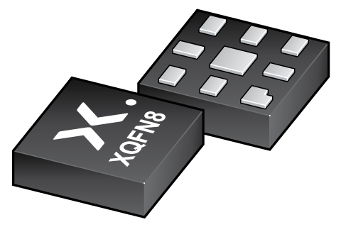
| 74LVCV2G66GM | XQFN8 |
PCB Symbol, Footprint and 3D Model
| Model Name | Description |
|---|---|
|
|
Package
All type numbers in the table below are discontinued.
| Type number | Orderable part number, (Ordering code (12NC)) | Status | Marking | Package | Package information | Reflow-/Wave soldering | Packing |
|---|---|---|---|---|---|---|---|
| 74LVCV2G66GM | 74LVCV2G66GM,125 (935281214125) |
Obsolete | Y66 |

XQFN8 (SOT902-2) |
SOT902-2 | SOT902-2_125 |
Environmental information
All type numbers in the table below are discontinued.
| Type number | Orderable part number | Chemical content | RoHS | RHF-indicator |
|---|---|---|---|---|
| 74LVCV2G66GM | 74LVCV2G66GM,125 | 74LVCV2G66GM |
|
|
Series
Documentation (4)
| File name | Title | Type | Date |
|---|---|---|---|
| Nexperia_document_guide_MiniLogic_MicroPak_201808 | MicroPak leadless logic portfolio guide | Brochure | 2018-09-03 |
| Nexperia_package_poster | Nexperia package poster | Leaflet | 2020-05-15 |
| XQFN8_SOT902-2_mk | plastic, extremely thin quad flat package; 8 terminals; 0.55 mm pitch; 1.6 mm x 1.6 mm x 0.5 mm body | Marcom graphics | 2017-01-28 |
| SOT902-2 | plastic, leadless extremely thin quad flat package; 8 terminals; 0.5 mm pitch; 1.6 mm x 1.6 mm x 0.5 mm body | Package information | 2020-04-21 |
Support
If you are in need of design/technical support, let us know and fill in the answer form we'll get back to you shortly.
Longevity
The Nexperia Longevity Program is aimed to provide our customers information from time to time about the expected time that our products can be ordered. The NLP is reviewed and updated regularly by our Executive Management Team. View our longevity program here.
Models
No documents available
PCB Symbol, Footprint and 3D Model
| Model Name | Description |
|---|---|
|
|
How does it work?
The interactive datasheets are based on the Nexperia MOSFET precision electrothermal models. With our interactive datasheets you can simply specify your own conditions interactively. Start by changing the values of the conditions. You can do this by using the sliders in the condition fields. By dragging the sliders you will see how the MOSFET will perform at the new conditions set.
