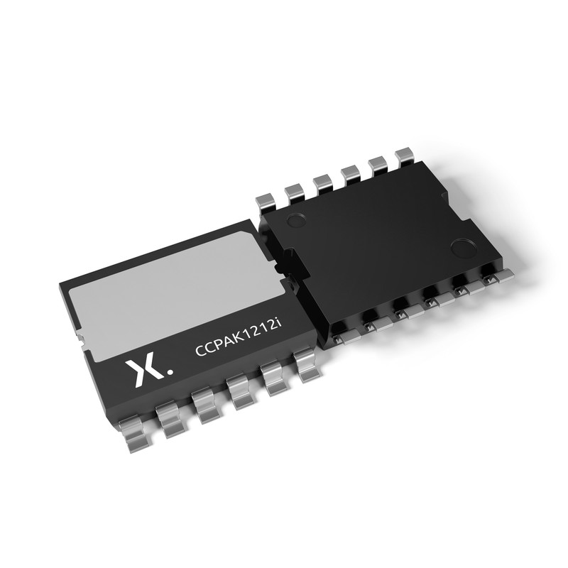
Top-side and bottom-side cooling
For added flexibility in designs and to further improve heat dissipation, CCPAK is available in both top-side cooling and traditional bottom-side cooling package designs.
The first in the portfolio of GaN SMD packages, the CCPAK1212 and CCPAK1212i have a compact footprint of only 12 x 12 mm and a low package height of 2.5 mm.
 |  |
CCPAK GaN FETs videos
Copper-clip SMD CCPAK GaN FET package in half-bridge evaluation board
Key features and benefits
Features and benefits
- Copper-clip
- 3 times lower inductances than industry-standard packages for lower switching losses and EMI
- Higher reliability compared to wire-bond solution
- Thermal performance
- Low Rth(j-mb) typ (<0.5 K/W) for optimal cooling
- 175 °C Tj max
- Manufacturability and robustness
- Flexible leads for temperature cycling reliability
- Flexible gull winged leads for robust board level reliability
- Compatible with SMD soldering and AOI
- Two cooling options
- Bottom-side cooling (CCPAK1212)
- Top-side cooling (CCPAK1212i)
- Plan for Qualifications
- AEC-Q101
- MSL1
- Halogen free
Key applications
Applications
- Automotive EV
- On board charging
- DC-to-DC converters
- Traction inverters
- Industrial
- Telecom and server Titanium grade power supplies
- Industrial vehicle charging
- Solar (PV) inverter
- AC servo drive / Frequency inverters
- Battery storage/UPS inverters
Parametric search
 Please wait loading data...
 Products
GaN FETs
| Type number | Description | Status | Quick access |
|---|---|---|---|
| GAN039-650NBB | 650 V, 33 mOhm Gallium Nitride (GaN) FET in a CCPAK1212 package | Production | |
| GAN039-650NTB | 650 V, 33 mOhm Gallium Nitride (GaN) FET in a CCPAK1212i package | Production |
Documentation
| File name | Title | Type | Date |
|---|---|---|---|
| AN90004.pdf | Probing considerations for fast switching applications | Application note | 2019-11-15 |
| AN90006.pdf | Circuit design and PCB layout recommendations for GaN FET half bridges | Application note | 2019-11-15 |
| RS3138_SOT8005_Combi_2_scr.jpg | CCPAK1212i (SOT8005) package image | Marcom graphics | 2020-05-26 |
| AN90005.pdf | Understanding Power GaN FET data sheet parameters | Application note | 2020-06-08 |
| TN90004.pdf | An insight into Nexperia Power GaN technology – Applications, quality, reliability and scalability | Technical note | 2020-07-21 |
| nexperia_whitepaper_gan_need_for_efficient_conversion.pdf | White paper: Power GaN technology: the need for efficient power conversion | White paper | 2020-07-23 |
| nexperia_whitepaper_gan_need_for_efficient_conversion_CHN.pdf | 白皮书: 功率GaN技术: 高效功率转换的需求 | White paper | 2020-08-17 |
| Nexperia_document_book_MOSFETGaNFETApplicationHandbook_2020.pdf | MOSFET & GaN FET Application Handbook | User manual | 2020-11-05 |
| nexperia_whitepaper_gan_need_for_efficient_conversion_Japanese.pdf | Whitepaper: GaN need for efficient conversion (Japanese) | White paper | 2021-05-20 |
| vp_CCPAK_GaN_FETs.zip | CCPAK GaN FETs (SMD) | Value proposition | 2022-01-27 |
| AN90030.pdf | Paralleling of Nexperia cascode GaN FETs in half-bridge topology | Application note | 2023-03-22 |
| Nexperia_Selection_guide_2023.pdf | Nexperia Selection Guide 2023 | Selection guide | 2023-05-10 |
| nexperia_document_leaflet_GaN_CCPAK_2023.pdf | CCPAK GaN FETs | Leaflet | 2023-10-25 |
| nexperia_document_leaflet_GaN_CCPAK_2023_CHN.pdf | CCPAK GaN FETs Chinese | Leaflet | 2023-10-25 |
| AN90053.pdf | Advanced SPICE models for Nexperia cascode Gallium Nitride (GaN) FETs | Application note | 2024-05-31 |
| nexperia_document_leaflet_GaNFETs_2024.pdf | Power GaN FETs | Leaflet | 2024-07-24 |
| nexperia_document_leaflet_GaNFETs_2024-CHN.pdf | Power GaN FETs Chinese | Leaflet | 2024-07-31 |
If you have a support question, let us know. If you are in need of design support, let us know and fill in the answer form, well get back to you shortly.
Or contact us for further support.