
74HC109-Q100; 74HCT109-Q100
Parametrics
| Type number | VCC (V) | Logic switching levels | Output drive capability (mA) | tpd (ns) | fmax (MHz) | Power dissipation considerations | Tamb (°C) | Package name | |||
|---|---|---|---|---|---|---|---|---|---|---|---|
| 74HC109D-Q100 | 2.0 - 6.0 | CMOS | ± 5.2 | 15 | 75 | low | -40~125 | SO16 | |||
| 74HCT109D-Q100 | 4.5 - 5.5 | TTL | ± 4 | 17 | 61 | low | -40~125 | 86 | 6.6 | 44 | SO16 |
| 74HCT109PW-Q100 | 4.5 - 5.5 | TTL | ± 4 | 17 | 61 | low | -40~125 | 119 | 3.2 | 48.1 | TSSOP16 |
Package
| Type number | Orderable part number, (Ordering code (12NC)) | Status | Marking | Package | Package information | Reflow-/Wave soldering | Packing |
|---|---|---|---|---|---|---|---|
| 74HC109D-Q100 | 74HC109D-Q100J (935334221118) |
Active | 74HC109D |
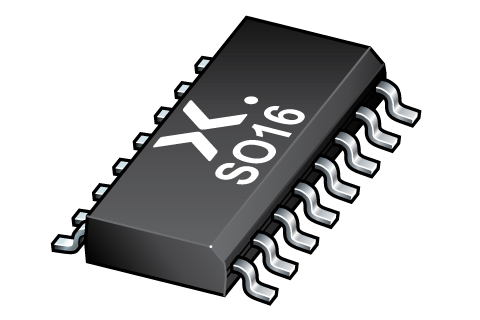
SO16 (SOT109-1) |
SOT109-1 |
SO-SOJ-REFLOW
SO-SOJ-WAVE WAVE_BG-BD-1 |
SOT109-1_118 |
| 74HCT109D-Q100 | 74HCT109D-Q100J (935332777118) |
Active | 74HCT109D |
SO16 (SOT109-1) |
SOT109-1 |
SO-SOJ-REFLOW
SO-SOJ-WAVE WAVE_BG-BD-1 |
SOT109-1_118 |
| 74HCT109PW-Q100 | 74HCT109PW-Q100J (935336488118) |
Active | HCT109 |
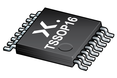
TSSOP16 (SOT403-1) |
SOT403-1 |
SSOP-TSSOP-VSO-WAVE
|
SOT403-1_118 |
Environmental information
| Type number | Orderable part number | Chemical content | RoHS | RHF-indicator |
|---|---|---|---|---|
| 74HC109D-Q100 | 74HC109D-Q100J | 74HC109D-Q100 |
|
|
| 74HCT109D-Q100 | 74HCT109D-Q100J | 74HCT109D-Q100 |
|
|
| 74HCT109PW-Q100 | 74HCT109PW-Q100J | 74HCT109PW-Q100 |
|
|
Documentation (14)
| File name | Title | Type | Date |
|---|---|---|---|
| 74HC_HCT109_Q100 | Dual JK flip-flop with set and reset; positive-edge-trigger | Data sheet | 2024-02-21 |
| AN11044 | Pin FMEA 74HC/74HCT family | Application note | 2019-01-09 |
| SOT109-1 | 3D model for products with SOT109-1 package | Design support | 2020-01-22 |
| SOT403-1 | 3D model for products with SOT403-1 package | Design support | 2020-01-22 |
| Nexperia_package_poster | Nexperia package poster | Leaflet | 2020-05-15 |
| SO16_SOT109-1_mk | plastic, small outline package; 16 leads; 1.27 mm pitch; 9.9 mm x 3.9 mm x 1.35 mm body | Marcom graphics | 2017-01-28 |
| TSSOP16_SOT403-1_mk | plastic, thin shrink small outline package; 16 leads; 0.65 mm pitch; 5 mm x 4.4 mm x 1.1 mm body | Marcom graphics | 2017-01-28 |
| SOT109-1 | plastic, small outline package; 16 leads; 1.27 mm pitch; 9.9 mm x 3.9 mm x 1.75 mm body | Package information | 2023-11-07 |
| SOT403-1 | plastic, thin shrink small outline package; 16 leads; 5 mm x 4.4 mm x 1.2 mm body | Package information | 2023-11-08 |
| SO-SOJ-REFLOW | Footprint for reflow soldering | Reflow soldering | 2009-10-08 |
| HCT_USER_GUIDE | HC/T User Guide | User manual | 1997-10-31 |
| SO-SOJ-WAVE | Footprint for wave soldering | Wave soldering | 2009-10-08 |
| WAVE_BG-BD-1 | Wave soldering profile | Wave soldering | 2021-09-08 |
| SSOP-TSSOP-VSO-WAVE | Footprint for wave soldering | Wave soldering | 2009-10-08 |
Support
If you are in need of design/technical support, let us know and fill in the answer form we'll get back to you shortly.
Ordering, pricing & availability
Sample
As a Nexperia customer you can order samples via our sales organization.
If you do not have a direct account with Nexperia our network of global and regional distributors is available and equipped to support you with Nexperia samples. Check out the list of official distributors.