Key features and benefits
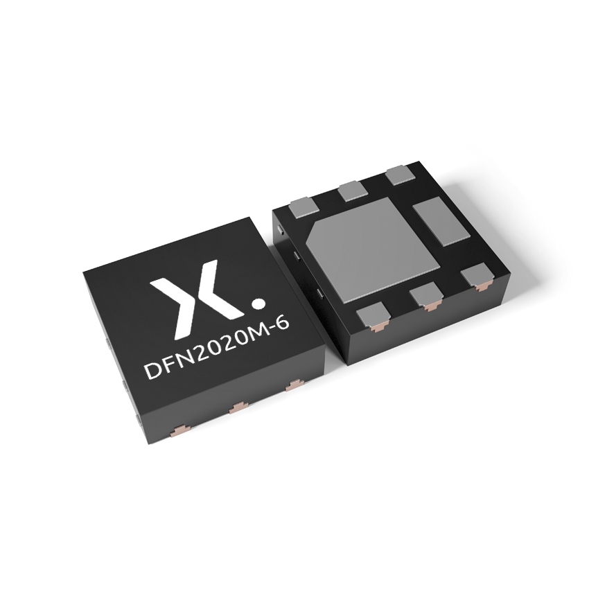
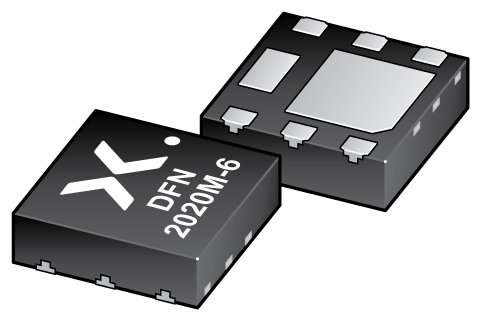
- Consumer version of the AEC-Q101 DFN2020MD-6 package, with footprint compatability
- Exposed drain pad for excellent thermal conduction
- Low RDS(on) for load switching e.g. smartphones
- Offering in N-Channel and P-Channel
- Low voltage drive (VGSth) typ - 0.7 V
- Voltage range of 12 V to 30 V
- Small height of only 0.65 mm
Applications
- Low RDS(on) load switching for e.g. smartphones
- DC/DC conversion
- Battery management
- Charging devices
- Solid state/hard drives
Featured products
Featured documents
Latest news and blogs
Latest videos
Nexperia’s Small-signal MOSFETs for portable and mobile applications
Parametric search
 Please wait loading data...
 Products
MOSFETs
| Type number | Description | Status | Quick access |
|---|---|---|---|
| PMPB12R5EP | 30 V, P-channel Trench MOSFET | EndOfLife | |
| PMPB12R7EP | 30 V, P-channel Trench MOSFET | Production | |
| PMPB07R3EN | 30 V, N-channel Trench MOSFET | Production | |
| PMPB17EP | 30 V, P-channel Trench MOSFET | Production | |
| PMPB50XN | 110 V, N-channel Trench MOSFET | Production | |
| PMPB09R5TP | 20 V, P-channel Trench MOSFET | EndOfLife | |
| PMPB10R3XN | 30 V, N-channel Trench MOSFET | Production | |
| PMPB07R3VP | 12 V, P-channel Trench MOSFET | EndOfLife | |
| PMPB14R0EP | 30 V, P-channel Trench MOSFET | EndOfLife | |
| PMPB08R4VP | 12 V, P-channel Trench MOSFET | EndOfLife | |
| PMPB11R2VP | 12 V, P-channel Trench MOSFET | EndOfLife | |
| PMPB16R5XNE | 30 V, N-channel Trench MOSFET | EndOfLife | |
| PMPB12R5UPE | 20 V, P-channel Trench MOSFET | EndOfLife | |
| PMPB14R7EP | 30 V, P-channel Trench MOSFET | EndOfLife | |
| PMPB09R1XN | 30 V, N-channel Trench MOSFET | EndOfLife | |
| PMPB09R5VP | 12 V, P-channel Trench MOSFET | EndOfLife | |
| PMPB14R8XN | 30 V, N-channel Trench MOSFET | EndOfLife | |
| PMPB08R5XN | 30 V, N-channel Trench MOSFET | EndOfLife | |
| PMPB08R6EN | 30 V, N-channel Trench MOSFET | EndOfLife | |
| PMPB07R0UN | 20 V, N-channel Trench MOSFET | EndOfLife | |
| PMPB19R0UPE | 20 V, P-channel Trench MOSFET | EndOfLife |
Documentation
| File name | Title | Type | Date |
|---|---|---|---|
| AN11119.pdf | Medium power small-signal MOSFETs in DC-to-DC conversion | Application note | 2013-05-07 |
| nexperia_report_aoi_inspection_dfn_201808.pdf | Automatic Optical Inspection of DFN Components | Report | 2018-09-03 |
| Nexperia_document_whitepaper_DFN_Wave_Soldering_2020.pdf | Whitepaper: Can DFNs be successfully wave soldered? | White paper | 2020-09-01 |
| AN90017.pdf | Load switches for mobile and computing applications | Application note | 2020-09-02 |
| AN90023.pdf | Thermal performance of DFN packages | Application note | 2020-11-23 |
| RS3383_DFN2020M-6_Combi.jpg | DFN2020M-6 3D MARCOM graphic | Marcom graphics | 2021-03-16 |
| vp_DFN2020M-6_MOSFETs.zip | DFN2020M-6 MOSFETs | Value proposition | 2021-03-22 |
| nexperia_document_leaflet_SsMOS_for_mobile_2022-CHN.pdf | 适合移动和便携式设备的 大批量小信号MOSFET, 采用WLCSP和无引脚DFN封装 | Leaflet | 2022-07-04 |
| nexperia_document_leaflet_SsMOS_for_mobile_2022.pdf | High volume small-signal MOSFETs for mobile and portables, in WLCSP and leadless DFN packages | Leaflet | 2022-07-04 |
Please contact us if you have any questions. If you are in need of design support, please fill in the answer form, we will get back to you shortly.
Please visit our contact us or {1} for further support.
