
74AXP4T245
4-bit dual supply translating transceiver; 3-state
The 74AXP4T245 is an 4-bit dual supply translating transceiver with 3-state outputs that enable bidirectional level translation. The device can be used as two 2-bit transceivers or as a 4-bit transceiver. It features four 2-bit input-output ports (nAn and nBn), a direction control input (nDIR), a output enable input (nOE) and dual supply pins (VCC(A) and VCC(B)). Both VCC(A) and VCC(B) can be supplied at any voltage between 0.9 V and 5.5 V making the device suitable for translating between any of the low voltage nodes (0.9 V, 1.2 V, 1.5 V, 1.8 V, 2.5 V, 3.3 V and 5.0 V). No power supply sequencing is required and output glitches during power supply transitions are prevented using patented circuitry. As a result glitches will not appear on the outputs for supply transitions during power-up/down between 20 mV/µs and 5.5 V/s.
Pins nAn, nOE and nDIR are referenced to VCC(A) and pins nBn are referenced to VCC(B). A HIGH on nDIR allows transmission from nAn to nBn and a LOW on nDIR allows transmission from nBn to nAn. The output enable input (nOE) can be used to disable the outputs so the buses are effectively isolated.
The device is fully specified for partial power-down applications using IOFF. The IOFF circuitry disables the output, preventing any damaging backflow current through the device when it is powered down. In suspend mode when either VCC(A) or VCC(B) are at GND level, both nAn and nBn are in the high-impedance OFF-state.
Features and benefits
Wide supply voltage range for VCC(A) and VCC(B): 0.9 V to 5.5 V
Low input capacitance; CI = 1.2 pF (typical)
Low output capacitance; CO = 3.6 pF (typical)
Low dynamic power consumption; CPD = 10 pF (typical)
Low static power consumption; ICC = 2 μA (25 °C maximum)
High noise immunity
Complies with JEDEC standard:
JESD8-12 (1.1 V to 1.3 V; inputs)
JESD8-11 (1.4 V to 1.6 V)
JESD8-7 (1.65 V to 1.95 V)
JESD8-5 (2.3 V to 2.7 V)
JESD8C (2.7 V to 3.6 V)
JESD12-6 (4.5 V to 5.5 V)
ESD protection:
HBM: ANSI/ESDA/JEDEC JS-001 class 2 exceeds 2 kV
CDM: ANSI/ESDA/JEDEC JS-002 class C3 exceeds 1 kV
Latch-up performance exceeds 100 mA per JESD78D Class II
Inputs accept voltages up to 5.5 V
-
Typical data rate figures:
320 Mbps when translating from 1.8 V to 3.3 V (up translation)
175 Mbps when translating from 3.3 V to 1.8 V (down translation)
Low noise overshoot and undershoot < 10% of VCCO
IOFF circuitry provides partial power-down mode operation
Specified from -40 °C to +125 °C
Parametrics
| Type number | VCC(A) (V) | VCC(B) (V) | Logic switching levels | Output drive capability (mA) | tpd (ns) | Nr of bits | Power dissipation considerations | Tamb (°C) | Package name |
|---|---|---|---|---|---|---|---|---|---|
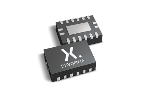
| 74AXP4T245BQ | 0.9 - 5.5 | 0.9 - 5.5 | CMOS | ± 12 | 9 | 4 | ultra low | -40~125 | DHVQFN16 |
| 74AXP4T245PW | 0.9 - 5.5 | 0.9 - 5.5 | CMOS | ± 12 | 9 | 4 | ultra low | -40~125 | TSSOP16 |
Package
| Type number | Orderable part number, (Ordering code (12NC)) | Status | Marking | Package | Package information | Reflow-/Wave soldering | Packing |
|---|---|---|---|---|---|---|---|
| 74AXP4T245BQ | 74AXP4T245BQX (935690704115) |
Active | P4T245 |
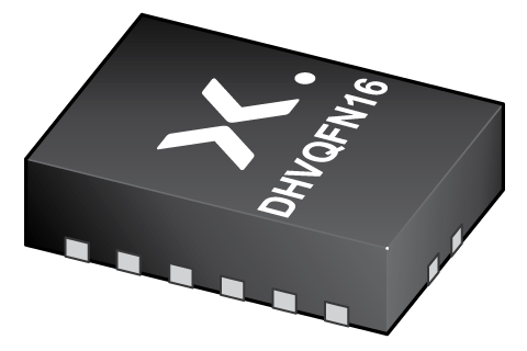
DHVQFN16 (SOT763-1) |
SOT763-1 | SOT763-1_115 | |
| 74AXP4T245PW | 74AXP4T245PWJ (935690703118) |
Active | XP4T245 |
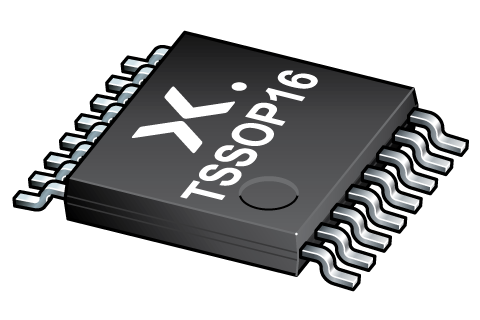
TSSOP16 (SOT403-1) |
SOT403-1 |
SSOP-TSSOP-VSO-WAVE
|
SOT403-1_118 |
Environmental information
| Type number | Orderable part number | Chemical content | RoHS | RHF-indicator |
|---|---|---|---|---|
| 74AXP4T245BQ | 74AXP4T245BQX | 74AXP4T245BQ |
|
|
| 74AXP4T245PW | 74AXP4T245PWJ | 74AXP4T245PW |
|
|
Documentation (11)
| File name | Title | Type | Date |
|---|---|---|---|
| 74AXP4T245 | 4-bit dual supply translating transceiver; 3-state | Data sheet | 2020-02-06 |
| AN90029 | Pin FMEA for AXPnT family | Application note | 2021-07-13 |
| SOT763-1 | 3D model for products with SOT763-1 package | Design support | 2019-10-03 |
| SOT403-1 | 3D model for products with SOT403-1 package | Design support | 2020-01-22 |
| Nexperia_package_poster | Nexperia package poster | Leaflet | 2020-05-15 |
| DHVQFN16_SOT763-1_mk | plastic, dual in-line compatible thermal enhanced very thin quad flat package; 16 terminals; 0.5 mm pitch; 3.5 mm x 2.5 mm x 0.85 mm body | Marcom graphics | 2017-01-28 |
| TSSOP16_SOT403-1_mk | plastic, thin shrink small outline package; 16 leads; 0.65 mm pitch; 5 mm x 4.4 mm x 1.1 mm body | Marcom graphics | 2017-01-28 |
| SOT763-1 | plastic, leadless dual in-line compatible thermal enhanced very thin quad flat package; 16 terminals; 0.5 mm pitch; 3.5 mm x 2.5 mm x 1 mm body | Package information | 2023-05-11 |
| SOT403-1 | plastic, thin shrink small outline package; 16 leads; 5 mm x 4.4 mm x 1.2 mm body | Package information | 2023-11-08 |
| Nexperia_Selection_guide_2023 | Nexperia Selection Guide 2023 | Selection guide | 2023-05-10 |
| SSOP-TSSOP-VSO-WAVE | Footprint for wave soldering | Wave soldering | 2009-10-08 |
Support
If you are in need of design/technical support, let us know and fill in the answer form we'll get back to you shortly.
Ordering, pricing & availability
Sample
As a Nexperia customer you can order samples via our sales organization.
If you do not have a direct account with Nexperia our network of global and regional distributors is available and equipped to support you with Nexperia samples. Check out the list of official distributors.