
Features and benefits
-
Wide supply voltage range:
-
VCC(A): 0.8 V to 3.6 V
-
VCC(B): 0.8 V to 3.6 V
-
-
High noise immunity
-
CMOS low power dissipation
-
Suspend mode
-
Latch-up performance exceeds 100 mA per JESD 78 Class II
-
Overvoltage tolerant inputs to 3.6 V
-
Dynamically controlled outputs
-
Low noise overshoot and undershoot < 10 % of VCC
-
IOFF circuitry provides partial Power-down mode operation
-
Maximum data rates:
-
500 Mbit/s (1.8 V to 3.3 V translation)
-
320 Mbit/s (< 1.8 V to 3.3 V translation)
-
320 Mbit/s (translate to 2.5 V or 1.8 V)
-
280 Mbit/s (translate to 1.5 V)
-
240 Mbit/s (translate to 1.2 V)
-
-
Complies with JEDEC standards:
-
JESD8-12 (0.8 V to 1.3 V)
-
JESD8-11 (0.9 V to 1.65 V)
-
JESD8-7 (1.65 V to 1.95 V)
-
JESD8-5 (2.3 V to 2.7 V)
-
JESD8C (2.7 V to 3.6 V)
-
-
ESD protection:
-
HBM: ANSI/ESDA/JEDEC JS-001 class 3B exceeds 8000 V
-
CDM: ANSI/ESDA/JEDEC JS-002 class C3 exceeds 1000 V
-
-
Multiple package options
-
Specified from -40 °C to +85 °C and -40 °C to +125 °C
Parametrics
| Type number | Product status | VCC(A) (V) | VCC(B) (V) | Logic switching levels | Output drive capability (mA) | tpd (ns) | Nr of bits | Power dissipation considerations | Tamb (°C) | Rth(j-a) (K/W) | Ψth(j-top) (K/W) | Rth(j-c) (K/W) | Package name | Category |
|---|---|---|---|---|---|---|---|---|---|---|---|---|---|---|
| 74AVC1T45GM | Production | 0.8 - 3.6 | 0.8 - 3.6 | CMOS/LVTTL | ± 12 | 2.1 | 1 | very low | -40~125 | 286 | 6.3 | 142 | XSON6 | Bi-directional | Direction controlled |
| 74AVC1T45GM-Q100 | Production | 0.8 - 3.6 | 0.8 - 3.6 | CMOS/LVTTL | ± 12 | 2.1 | 1 | very low | -40~125 | 286 | 6.3 | 142 | XSON6 | Bi-directional | Direction controlled |
| 74AVC1T45GN | Production | 0.8 - 3.6 | 0.8 - 3.6 | CMOS/LVTTL | ± 12 | 2.1 | 1 | very low | -40~125 | 264 | 9.7 | 164 | XSON6 | Bi-directional | Direction controlled |
| 74AVC1T45GS | Production | 0.8 - 3.6 | 0.8 - 3.6 | CMOS/LVTTL | ± 12 | 2.1 | 1 | very low | -40~125 | 262 | 12.2 | 170 | XSON6 | Bi-directional | Direction controlled |
| 74AVC1T45GS-Q100 | Production | 0.8 - 3.6 | 0.8 - 3.6 | CMOS/LVTTL | ± 12 | 2.1 | 1 | very low | -40~125 | 262 | 12.2 | 170 | XSON6 | Bi-directional | Direction controlled |
| 74AVC1T45GW | Production | 0.8 - 3.6 | 0.8 - 3.6 | CMOS/LVTTL | ± 12 | 2.1 | 1 | very low | -40~125 | 262 | 36.1 | 150 | TSSOP6 | Bi-directional | Direction controlled |
| 74AVC1T45GW-Q100 | Production | 0.8 - 3.6 | 0.8 - 3.6 | CMOS/LVTTL | ± 12 | 2.1 | 1 | very low | -40~125 | 262 | 36.1 | 150 | TSSOP6 | Bi-directional | Direction controlled |
| 74AVC1T45GX | Production | 0.8 - 3.6 | 0.8 - 3.6 | CMOS/LVTTL | ± 12 | 2.1 | 1 | very low | -40~125 | 470 | 14.6 | 238 | X2SON6 | Bi-directional | Direction controlled |
Package
| Type number | Package | Package information | Reflow-/Wave soldering | Packing | Status | Marking | Orderable part number, (Ordering code (12NC)) |
|---|---|---|---|---|---|---|---|
| 74AVC1T45GM | 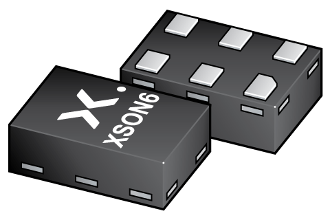 XSON6 (SOT886) | SOT886 | REFLOW_BG-BD-1 | SOT886_132 | Active | B5 | 74AVC1T45GM,132 ( 9352 841 54132 ) |
| SOT886_115 | Active | B5 | 74AVC1T45GM,115 ( 9352 841 54115 ) | ||||
| 74AVC1T45GM-Q100 | XSON6 (SOT886) | SOT886 | REFLOW_BG-BD-1 | SOT886_125 | Active | B5 | 74AVC1T45GM-Q100H ( 9352 994 89125 ) |
| 74AVC1T45GN | 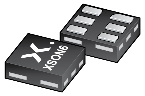 XSON6 (SOT1115) | SOT1115 | REFLOW_BG-BD-1 | SOT1115_132 | Active | B5 | 74AVC1T45GN,132 ( 9352 943 59132 ) |
| 74AVC1T45GS | 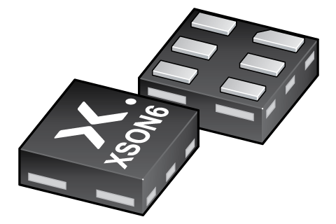 XSON6 (SOT1202) | SOT1202 | REFLOW_BG-BD-1 | SOT1202_132 | Active | B5 | 74AVC1T45GS,132 ( 9352 943 61132 ) |
| 74AVC1T45GS-Q100 | XSON6 (SOT1202) | SOT1202 | REFLOW_BG-BD-1 | SOT1202_125 | Active | B5 | 74AVC1T45GS-Q100H ( 9356 907 71125 ) |
| 74AVC1T45GW | 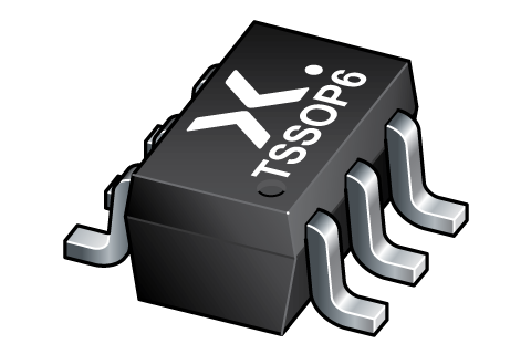 TSSOP6 (SOT363-2) | SOT363-2 | SOT363-2_125 | Active | B5 | 74AVC1T45GW,125 ( 9352 841 53125 ) | |
| 74AVC1T45GW-Q100 | TSSOP6 (SOT363-2) | SOT363-2 | SOT363-2_125 | Active | B5 | 74AVC1T45GW-Q100H ( 9352 994 91125 ) | |
| 74AVC1T45GX | 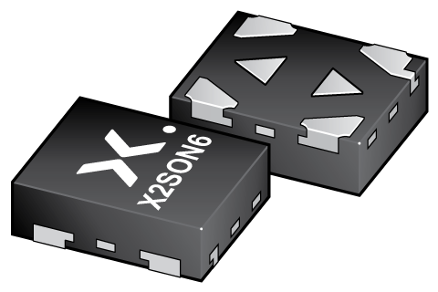 X2SON6 (SOT1255-2) | SOT1255-2 | SOT1255-2_147 | Active | B5 | 74AVC1T45GXZ ( 9353 084 68147 ) |
Environmental information
| Type number | Orderable part number | Chemical content | RoHS | RHF-indicator | Leadfree conversion date |
|---|---|---|---|---|---|
| 74AVC1T45GM | 74AVC1T45GM,132 | 74AVC1T45GM | Always Pb-free | ||
| 74AVC1T45GM | 74AVC1T45GM,115 | 74AVC1T45GM | Always Pb-free | ||
| 74AVC1T45GM-Q100 | 74AVC1T45GM-Q100H | 74AVC1T45GM-Q100 | Always Pb-free | ||
| 74AVC1T45GN | 74AVC1T45GN,132 | 74AVC1T45GN | Always Pb-free | ||
| 74AVC1T45GS | 74AVC1T45GS,132 | 74AVC1T45GS | Always Pb-free | ||
| 74AVC1T45GS-Q100 | 74AVC1T45GS-Q100H | 74AVC1T45GS-Q100 | week 25, 2019 | ||
| 74AVC1T45GW | 74AVC1T45GW,125 | 74AVC1T45GW | Always Pb-free | ||
| 74AVC1T45GW-Q100 | 74AVC1T45GW-Q100H | 74AVC1T45GW-Q100 | Always Pb-free | ||
| 74AVC1T45GX | 74AVC1T45GXZ | 74AVC1T45GX | week 25, 2019 |
Documentation (17)
| File name | Title | Type | Date |
|---|---|---|---|
| 74AVC1T45 | Dual-supply voltage level translator/transceiver; 3-state | Data sheet | 2024-07-02 |
| AN10161 | PicoGate Logic footprints | Application note | 2002-10-29 |
| Nexperia_document_guide_Logic_translators | Nexperia Logic Translators | Brochure | 2021-04-12 |
| avc1t45 | 74AVC1T45 IBIS model | IBIS model | 2016-02-24 |
| Nexperia_document_leaflet_Logic_X2SON_packages_062018 | X2SON ultra-small 4, 5, 6 & 8-pin leadless packages | Leaflet | 2018-06-05 |
| Nexperia_Selection_guide_2023 | Nexperia Selection Guide 2023 | Selection guide | 2023-05-10 |
| REFLOW_BG-BD-1 | Reflow soldering profile | Reflow soldering | 2021-04-06 |
| MAR_SOT1202 | MAR_SOT1202 Topmark | Top marking | 2013-06-03 |
| SOT1202 | plastic, leadless extremely thin small outline package; 6 terminals; 0.35 mm pitch; 1 mm x 1mm x 0.35 mm body | Package information | 2022-06-01 |
| SOT363-2 | plastic thin shrink small outline package; 6 leads; body width 1.25 mm | Package information | 2022-11-21 |
| SOT1255-2 | plastic thermal enhanced extremely thin small outline package; no leads;6 terminals; body 1.0 x 0.8 x 0.32 mm | Package information | 2020-08-27 |
| REFLOW_BG-BD-1 | Reflow soldering profile | Reflow soldering | 2021-04-06 |
| MAR_SOT1115 | MAR_SOT1115 Topmark | Top marking | 2013-06-03 |
| SOT1115 | plastic, leadless extremely thin small outline package; 6 terminals; 0.3 mm pitch; 0.9 mm x 1 mm x 0.35 mm body | Package information | 2022-05-27 |
| MAR_SOT886 | MAR_SOT886 Topmark | Top marking | 2013-06-03 |
| SOT886 | plastic, leadless extremely thin small outline package; 6 terminals; 0.5 mm pitch; 1 mm x 1.45 mm x 0.5 mm body | Package information | 2022-06-01 |
| REFLOW_BG-BD-1 | Reflow soldering profile | Reflow soldering | 2021-04-06 |
Support
If you are in need of design/technical support, let us know and fill in the answer form, we'll get back to you shortly.
Models
| File name | Title | Type | Date |
|---|---|---|---|
| avc1t45 | 74AVC1T45 IBIS model | IBIS model | 2016-02-24 |
Ordering, pricing & availability
Sample
As a Nexperia customer you can order samples via our sales organization.
If you do not have a direct account with Nexperia our network of global and regional distributors is available and equipped to support you with Nexperia samples. Check out the list of official distributors.