Features and benefits
-
Automotive product qualification in accordance with AEC-Q100 (Grade 1)
-
Specified from -40 °C to +85 °C and from -40 °C to +125 °C
-
-
Wide supply voltage range from 1.0 to 5.5 V
-
CMOS low power dissipation
-
Latch-up performance exceeds 100 mA per JESD 78 Class II Level B
-
Optimized for low voltage applications: 1.0 V to 3.6 V
-
Accepts TTL input levels between VCC = 2.7 V and VCC = 3.6 V
-
Typical output ground bounce < 0.8 V at VCC = 3.3 V and Tamb = 25 °C
-
Typical HIGH-level output voltage (VOH) undershoot: > 2 V at VCC = 3.3 V and Tamb = 25 °C
-
Complies with JEDEC standards:
- JESD8-7 (1.65 V to 1.95 V)
- JESD8-5 (2.3 V to 2.7 V)
- JESD8C (2.7 V to 3.6 V)
- JESD36 (4.5 V to 5.5 V)
-
ESD protection:
-
HBM: ANSI/ESDA/JEDEC JS-001 class 2 exceeds 2000 V
-
CDM: ANSI/ESDA/JEDEC JS-002 class C3 exceeds 1000 V
-
Parametrics
| Type number | Product status | VCC (V) | Logic switching levels | Output drive capability (mA) | tpd (ns) | fmax (MHz) | Nr of bits | Power dissipation considerations | Tamb (°C) | Rth(j-a) (K/W) | Ψth(j-top) (K/W) | Rth(j-c) (K/W) | Package name |
|---|---|---|---|---|---|---|---|---|---|---|---|---|---|
| 74LV00D-Q100 | Production | 1.0 - 5.5 | TTL | ± 12 | 7 | 30 | 4 | low | -40~125 | 93 | 10.3 | 51 | SO14 |
| 74LV00PW-Q100 | Production | 1.0 - 5.5 | TTL | ± 12 | 7 | 30 | 4 | low | -40~125 | 131 | 4.5 | 56.3 | TSSOP14 |
Package
| Type number | Package | Package information | Reflow-/Wave soldering | Packing | Status | Marking | Orderable part number, (Ordering code (12NC)) |
|---|---|---|---|---|---|---|---|
| 74LV00D-Q100 | 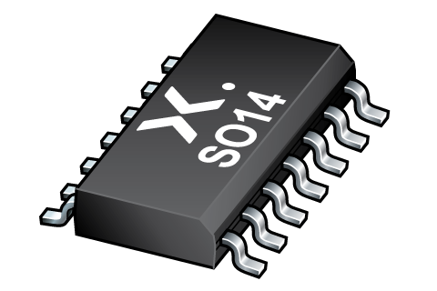 SO14 (SOT108-1) | SOT108-1 | SO-SOJ-REFLOW SO-SOJ-WAVE | SOT108-1_118 | Active | 74LV00D | 74LV00D-Q100J ( 9356 916 20118 ) |
| 74LV00PW-Q100 | 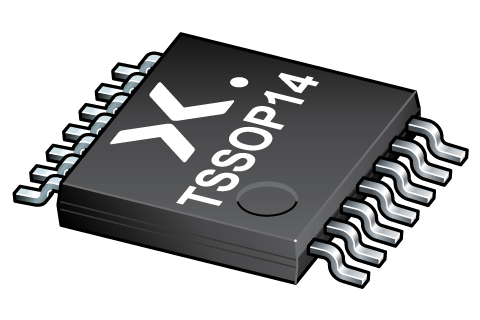 TSSOP14 (SOT402-1) | SOT402-1 | SSOP-TSSOP-VSO-WAVE | SOT402-1_118 | Active | LV00 | 74LV00PW-Q100J ( 9356 915 83118 ) |
Environmental information
| Type number | Orderable part number | Chemical content | RoHS | RHF-indicator | Leadfree conversion date |
|---|---|---|---|---|---|
| 74LV00D-Q100 | 74LV00D-Q100J | 74LV00D-Q100 | |||
| 74LV00PW-Q100 | 74LV00PW-Q100J | 74LV00PW-Q100 |
Documentation (7)
| File name | Title | Type | Date |
|---|---|---|---|
| 74LV00_Q100 | Quad 2-input NAND gate | Data sheet | 2024-01-22 |
| SOT402-1 | plastic, thin shrink small outline package; 14 leads; 0.65 mm pitch; 5 mm x 4.4 mm x 1.2 mm body | Package information | 2023-11-07 |
| SSOP-TSSOP-VSO-WAVE | Footprint for wave soldering | Wave soldering | 2009-10-08 |
| SO-SOJ-WAVE | Footprint for wave soldering | Wave soldering | 2009-10-08 |
| SO-SOJ-REFLOW | Footprint for reflow soldering | Reflow soldering | 2009-10-08 |
| WAVE_BG-BD-1 | Wave soldering profile | Wave soldering | 2021-09-08 |
| SOT108-1 | plastic, small outline package; 14 leads; 1.27 mm pitch; 8.65 mm x 3.9 mm x 1.75 mm body | Package information | 2023-11-07 |
Support
If you are in need of design/technical support, let us know and fill in the answer form, we'll get back to you shortly.
Ordering, pricing & availability
Sample
As a Nexperia customer you can order samples via our sales organization.
If you do not have a direct account with Nexperia our network of global and regional distributors is available and equipped to support you with Nexperia samples. Check out the list of official distributors.