
NMUX1308
1.5 V to 5.5 V, 8-channel analog switch multiplexer and demultiplexer with injection-current control
The NMUX1308 is a general purpose, CMOS, bi-directional, 8 channel analog switch, with an operating voltage range of 1.5 V to 5.5 V. The NMUX1308 is dual source compatible with existing 4851 and 4051 devices. The NMUX1308 extends the digital logic thresholds to be compatible with 1.8 V systems without the need for voltage translation.
The analog signal pins are comprised of a common input/output (Z) and eight independent inputs/outputs (Y0 to Y7). All analog signal pins are bi-directional and support a voltage range from GND to VCC.
All analog signal pins integrate injection current control circuitry. This control circuitry isolates overvoltage spikes on disconnected analog signal pins from coupling to the connected analog signal path, thereby preserving measurement accuracy. Additionally, this integration makes the use of external overvoltage clamp components (e.g. resistive diode network) unnecessary.
There are four control signal pins (S0, S1, S2, and E). S0, S1, and S2 determine the analog channels to connect between Z and Yn. E can be used to override S0, S1, and S2, disconnecting all analog channels.
The control signal pins support 1.8 V logic thresholds across all operating voltages. In addition, these pins are 5.5 V tolerant, enabling up to 5.5 V operation independent of supply voltage.
Features and benefits
SP8T-Z functionality
Wide operating range: 1.5 V to 5.5 V
Rail-to-Rail operation on analog signal pins
Injection current control
-
1.8 V digital logic thresholds
Digital pins compatible with 1.8 V logic thresholds across full VCC range
Removes need for up-translation device for compatibility with low voltage GPIOs
Ioff circuitry
Enables wider latitude for power sequencing considerations
Isolates backflow between supply rail and any biased digital/analog input when VCC = 0 V
Prevents any biased digital/analog input from backpowering VCC when VCC = 0 V
Maintains Hi-Z state of analog switch when VCC = 0 V
-
5.5 V overvoltage tolerant digital inputs
Supports switching of 5.5 V digital signals across full VCC operating range
Removes need for down-translation when switching thresholds are met
Pin compatible with industry standard 4051 and 4851 analog switch products
-
ESD protection:
HBM: ANSI/ESDA/JEDEC JS-001 class 2 exceeds 2000 V
CDM: ANSI/ESDA/JEDEC JS-002 class C2b exceeds 750 V
- Specified from -40 °C to +85 °C and from -40 °C to +125 °C
Applications
Analog or digital multiplexing/demultiplexing
System monitoring and diagnostics
Enterprise computing
Appliances
Parametrics
| Type number | Configuration | VCC (V) | Logic switching levels | RON (Ω) | RON(FLAT) (Ω) | f(-3dB) (MHz) | THD (%) | Xtalk (dB) | Power dissipation considerations | Tamb (°C) | Package name |
|---|---|---|---|---|---|---|---|---|---|---|---|
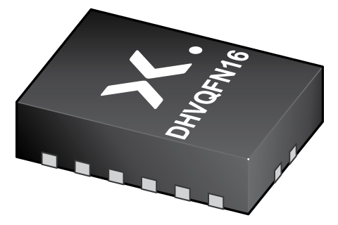
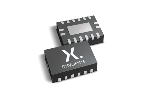
| NMUX1308BQ | SP8T-Z | 1.5 - 5.5 | CMOS | 60 | - | 325 | - | -105 | very low | -40~125 | DHVQFN16 |
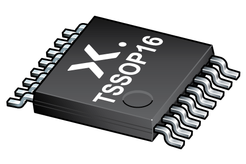
| NMUX1308PW | SP8T-Z | 1.5 - 5.5 | CMOS | 60 | - | 325 | - | -105 | very low | -40~125 | TSSOP16 |
Package
| Type number | Orderable part number, (Ordering code (12NC)) | Status | Marking | Package | Package information | Reflow-/Wave soldering | Packing |
|---|---|---|---|---|---|---|---|
| NMUX1308BQ | NMUX1308BQX (935691411115) |
Active | NM1308 |
DHVQFN16 (SOT763-1) |
SOT763-1 | SOT763-1_115 | |
| NMUX1308PW | NMUX1308PWJ (935691413118) |
Active | NMU1308 |
TSSOP16 (SOT403-1) |
SOT403-1 |
SSOP-TSSOP-VSO-WAVE
|
SOT403-1_118 |
Environmental information
| Type number | Orderable part number | Chemical content | RoHS | RHF-indicator |
|---|---|---|---|---|
| NMUX1308BQ | NMUX1308BQX | NMUX1308BQ |
|
|
| NMUX1308PW | NMUX1308PWJ | NMUX1308PW |
|
|
Documentation (12)
| File name | Title | Type | Date |
|---|---|---|---|
| NMUX1308 | 1.5 V to 5.5 V, 8-channel analog switch multiplexer and demultiplexer with injection-current control | Data sheet | 2024-07-25 |
| AN90051 | Pin FMEA for NMUX130x family | Application note | 2024-02-13 |
| SOT763-1 | 3D model for products with SOT763-1 package | Design support | 2019-10-03 |
| SOT403-1 | 3D model for products with SOT403-1 package | Design support | 2020-01-22 |
| 1_8V_General_purpose_injection_control_analog_switch_leaflet | 1.8 V General purpose SP8T-Z and 2x SP4T-Z analog switches with injection current control | Leaflet | 2024-03-05 |
| Nexperia_package_poster | Nexperia package poster | Leaflet | 2020-05-15 |
| DHVQFN16_SOT763-1_mk | plastic, dual in-line compatible thermal enhanced very thin quad flat package; 16 terminals; 0.5 mm pitch; 3.5 mm x 2.5 mm x 0.85 mm body | Marcom graphics | 2017-01-28 |
| TSSOP16_SOT403-1_mk | plastic, thin shrink small outline package; 16 leads; 0.65 mm pitch; 5 mm x 4.4 mm x 1.1 mm body | Marcom graphics | 2017-01-28 |
| SOT763-1 | plastic, leadless dual in-line compatible thermal enhanced very thin quad flat package; 16 terminals; 0.5 mm pitch; 3.5 mm x 2.5 mm x 1 mm body | Package information | 2023-05-11 |
| SOT403-1 | plastic, thin shrink small outline package; 16 leads; 5 mm x 4.4 mm x 1.2 mm body | Package information | 2023-11-08 |
| UM90026 | NMUX1308; NMUX1309 evaluation board | User manual | 2024-04-30 |
| SSOP-TSSOP-VSO-WAVE | Footprint for wave soldering | Wave soldering | 2009-10-08 |
Support
If you are in need of design/technical support, let us know and fill in the answer form we'll get back to you shortly.
Ordering, pricing & availability
Sample
As a Nexperia customer you can order samples via our sales organization.
If you do not have a direct account with Nexperia our network of global and regional distributors is available and equipped to support you with Nexperia samples. Check out the list of official distributors.