
74AVC8T245-Q100
8-bit dual supply translating transceiver with configurable voltage translation; 3-state
The 74AVC8T245-Q100 is an 8-bit, dual supply transceiver that enables bidirectional level translation. It features two 8-bit input-output ports (An and Bn), a direction control input (DIR), an output enable input (OE) and dual supply pins (VCC(A) and VCC(B)). Both VCC(A) and VCC(B) can be supplied at any voltage between 0.8 V and 3.6 V making the device suitable for translating between any of the low voltage nodes (0.8 V, 1.2 V, 1.5 V, 1.8 V, 2.5 V and 3.3 V). Pins An, OE and DIR are referenced to VCC(A) and pins Bn are referenced to VCC(B). A HIGH on DIR allows transmission from An to Bn and a LOW on DIR allows transmission from Bn to An. The output enable input (OE) can be used to disable the outputs so the buses are effectively isolated.
The device is fully specified for partial power-down applications using IOFF. The IOFF circuitry disables the output, preventing any damaging backflow current through the device when it is powered down. In suspend mode when either VCC(A) or VCC(B) are at GND level, both An and Bn are in the high-impedance OFF-state.
This product has been qualified to the Automotive Electronics Council (AEC) standard Q100 (Grade 1) and is suitable for use in automotive applications.
Features and benefits
Automotive product qualification in accordance with AEC-Q100 (Grade 1)
Specified from -40 °C to +85 °C and from -40 °C to +125 °C
Wide supply voltage range: VCC(A): 0.8 V to 3.6 V; VCC(B): 0.8 V to 3.6 V
Complies with JEDEC standards:
JESD8-12 (0.8 V to 1.3 V)
JESD8-11 (0.9 V to 1.65 V)
JESD8-7 (1.2 V to 1.95 V)
JESD8-5 (1.8 V to 2.7 V)
JESD8-B (2.7 V to 3.6 V)
Maximum data rates:
380 Mbit/s (≥ 1.8 V to 3.3 V translation)
260 Mbit/s (≥ 1.1 V to 3.3 V translation)
260 Mbit/s (≥ 1.1 V to 2.5 V translation)
210 Mbit/s (≥ 1.1 V to 1.8 V translation)
150 Mbit/s (≥ 1.1 V to 1.5 V translation)
100 Mbit/s (≥ 1.1 V to 1.2 V translation)
Suspend mode
Latch-up performance exceeds 100 mA per JESD 78 Class II
Inputs accept voltages up to 3.6 V
IOFF circuitry provides partial Power-down mode operation
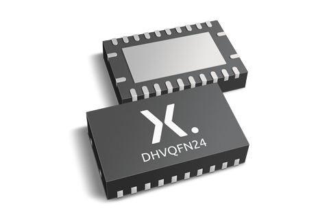
DHVQFN package with Side-Wettable Flanks enabling Automated Optical Inspection (AOI) of solder joints
ESD protection:
HBM: ANSI/ESDA/JEDEC JS-001 class 3B exceeds 8000 V
CDM: ANSI/ESDA/JEDEC JS-002 class C3 exceeds 1000 V
Parametrics
| Type number | VCC(A) (V) | VCC(B) (V) | Logic switching levels | Output drive capability (mA) | tpd (ns) | Nr of bits | Power dissipation considerations | Tamb (°C) | Package name |
|---|---|---|---|---|---|---|---|---|---|
| 74AVC8T245BQ-Q100 | 0.8 - 3.6 | 0.8 - 3.6 | CMOS/LVTTL | ± 12 | 2.1 | 8 | very low | -40~125 | DHVQFN24 |
| 74AVC8T245PW-Q100 | 0.8 - 3.6 | 0.8 - 3.6 | CMOS/LVTTL | ± 12 | 2.1 | 8 | very low | -40~125 | TSSOP24 |
Package
| Type number | Orderable part number, (Ordering code (12NC)) | Status | Marking | Package | Package information | Reflow-/Wave soldering | Packing |
|---|---|---|---|---|---|---|---|
| 74AVC8T245BQ-Q100 | 74AVC8T245BQ-Q100J (935300551118) |
Active | AVC8T245 |
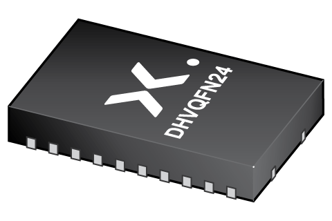
DHVQFN24 (SOT815-1) |
SOT815-1 | SOT815-1_118 | |
| 74AVC8T245PW-Q100 | 74AVC8T245PW-Q100J (935300549118) |
Active | AVC8T245 |
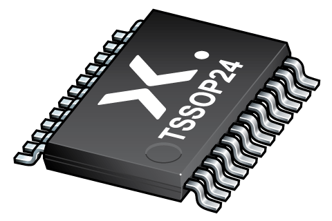
TSSOP24 (SOT355-1) |
SOT355-1 |
SSOP-TSSOP-VSO-WAVE
|
SOT355-1_118 |
Environmental information
| Type number | Orderable part number | Chemical content | RoHS | RHF-indicator |
|---|---|---|---|---|
| 74AVC8T245BQ-Q100 | 74AVC8T245BQ-Q100J | 74AVC8T245BQ-Q100 |
|
|
| 74AVC8T245PW-Q100 | 74AVC8T245PW-Q100J | 74AVC8T245PW-Q100 |
|
|
Documentation (10)
| File name | Title | Type | Date |
|---|---|---|---|
| 74AVC8T245_Q100 | 8-bit dual supply translating transceiver with configurable voltage translation; 3-state | Data sheet | 2024-06-25 |
| SOT815-1 | 3D model for products with SOT815-1 package | Design support | 2019-10-03 |
| SOT355-1 | 3D model for products with SOT355-1 package | Design support | 2020-01-22 |
| avc8t245 | avc8t245 IBIS model | IBIS model | 2021-02-02 |
| Nexperia_package_poster | Nexperia package poster | Leaflet | 2020-05-15 |
| DHVQFN24_SOT815-1_mk | plastic, dual in-line compatible thermal enhanced very thin quad flat package; 24 terminals; 0.5 mm pitch; 3.5 mm x 5.5 mm x 0.85 mm body | Marcom graphics | 2017-01-28 |
| SOT815-1 | plastic, leadless dual in-line compatible thermal enhanced very thin quad flat package; 24 terminals; 0.5 mm pitch; 5.5 mm x 3.5 mm x 1 mm body | Package information | 2021-08-17 |
| SOT355-1 | plastic, thin shrink small outline package; 24 leads; 0.65 mm pitch; 7.8 mm x 4.4 mm x 1.1 mm body | Package information | 2022-06-22 |
| Nexperia_Selection_guide_2023 | Nexperia Selection Guide 2023 | Selection guide | 2023-05-10 |
| SSOP-TSSOP-VSO-WAVE | Footprint for wave soldering | Wave soldering | 2009-10-08 |
Support
If you are in need of design/technical support, let us know and fill in the answer form we'll get back to you shortly.
Ordering, pricing & availability
Sample
As a Nexperia customer you can order samples via our sales organization.
If you do not have a direct account with Nexperia our network of global and regional distributors is available and equipped to support you with Nexperia samples. Check out the list of official distributors.