74LV4051-Q100
8-channel analog multiplexer/demultiplexer
The 74LV4051-Q100 is an 8-channel analog multiplexer/demultiplexer with three digital select inputs (S0 to S2), an active-LOW enable input (E), eight independent inputs/outputs (Y0 to Y7) and a common input/output (Z). It is a low-voltage Si-gate CMOS device that is pin and function compatible with 74HC4051 and 74HCT4051. With E LOW, one of the eight switches is selected (low impedance ON-state) by S0 to S2. With E HIGH, all switches are in the high-impedance OFF-state, independent of S0 to S2.
VCC and GND are the supply voltage pins for the digital control inputs (S0 to S2, and E). The VCC to GND ranges are 1.0 V to 6.0 V. The analog inputs/outputs (Y0 to Y7, and Z) can swing between VCC as a positive limit and VEE as a negative limit. VCC - VEE may not exceed 6.0 V. For operation as a digital multiplexer/demultiplexer, VEE is connected to GND (typically ground).
This product has been qualified to the Automotive Electronics Council (AEC) standard Q100 (Grade 1) and is suitable for use in automotive applications.
Features and benefits
Automotive product qualification in accordance with AEC-Q100 (Grade 1)
Specified from -40 °C to +85 °C and from -40 °C to +125 °C
Optimized for low-voltage applications: 1.0 V to 6.0 V
Accepts TTL input levels between VCC = 2.7 V and VCC = 3.6 V
Low ON resistance:
145 Ω (typical) at VCC - VEE = 2.0 V
80 Ω (typical) at VCC - VEE = 3.0 V
60 Ω (typical) at VCC - VEE = 4.5 V
Logic level translation:
To enable 3 V logic to communicate with ±3 V analog signals
Typical ‘break before make’ built in
ESD protection:
HBM: ANSI/ESDA/JEDEC JS-001 class 2 exceeds 2000 V
CDM: ANSI/ESDA/JEDEC JS-002 class C3 exceeds 1000 V
Parametrics
| Type number | Configuration | VCC (V) | RON (Ω) | Logic switching levels | Power dissipation considerations | Tamb (°C) | Package name |
|---|---|---|---|---|---|---|---|
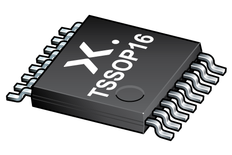
| 74LV4051PW-Q100 | SP8T-Z | 1.0 - 6.0 | 135 | TTL | very low | -40~125 | TSSOP16 |
Package
| Type number | Orderable part number, (Ordering code (12NC)) | Status | Marking | Package | Package information | Reflow-/Wave soldering | Packing |
|---|---|---|---|---|---|---|---|
| 74LV4051PW-Q100 | 74LV4051PW-Q100J (935691250118) |
Active | LV4051 |
TSSOP16 (SOT403-1) |
SOT403-1 |
SSOP-TSSOP-VSO-WAVE
|
SOT403-1_118 |
Environmental information
| Type number | Orderable part number | Chemical content | RoHS | RHF-indicator |
|---|---|---|---|---|
| 74LV4051PW-Q100 | 74LV4051PW-Q100J | 74LV4051PW-Q100 |
|
|
Documentation (8)
| File name | Title | Type | Date |
|---|---|---|---|
| 74LV4051_Q100 | 8-channel analog multiplexer/demultiplexer | Data sheet | 2024-03-29 |
| sv01705 | Block diagram: 74LV4051D, 74LV4051DB, 74LV4051N, 74LV4051PW | Block diagram | 2009-11-04 |
| SOT403-1 | 3D model for products with SOT403-1 package | Design support | 2020-01-22 |
| Nexperia_package_poster | Nexperia package poster | Leaflet | 2020-05-15 |
| TSSOP16_SOT403-1_mk | plastic, thin shrink small outline package; 16 leads; 0.65 mm pitch; 5 mm x 4.4 mm x 1.1 mm body | Marcom graphics | 2017-01-28 |
| SOT403-1 | plastic, thin shrink small outline package; 16 leads; 5 mm x 4.4 mm x 1.2 mm body | Package information | 2023-11-08 |
| lv | lv Spice model | SPICE model | 2013-05-07 |
| SSOP-TSSOP-VSO-WAVE | Footprint for wave soldering | Wave soldering | 2009-10-08 |
Support
If you are in need of design/technical support, let us know and fill in the answer form we'll get back to you shortly.
Ordering, pricing & availability
Sample
As a Nexperia customer you can order samples via our sales organization.
If you do not have a direct account with Nexperia our network of global and regional distributors is available and equipped to support you with Nexperia samples. Check out the list of official distributors.