
74LV4094
8-stage shift-and-store bus register
The 74LV4094 is an 8-bit serial-in/serial or parallel-out shift register with a storage register and 3-state outputs. Both the shift and storage register have separate clocks. The device features a serial input (D) and two serial outputs (QS1 and QS2) to enable cascading. Data is shifted on the LOW-to-HIGH transitions of the CP input. Data is available at QS1 on the LOW-to-HIGH transitions of the CP input to allow cascading when clock edges are fast. The same data is available at QS2 on the next HIGH-to-LOW transition of the CP input to allow cascading when clock edges are slow. The data in the shift register is transferred to the storage register when the STR input is HIGH. Data in the storage register appears at the outputs whenever the output enable input (OE) is HIGH. A LOW on OE causes the outputs to assume a high-impedance OFF-state. Operation of the OE input does not affect the state of the registers. Inputs include clamp diodes. This enables the use of current limiting resistors to interface inputs to voltages in excess VCC.
Features and benefits
Optimized for low voltage applications over a wide supply voltage range from 1.0 V to 3.6 V
Accepts TTL input levels between VCC = 2.7 V and VCC = 3.6 V
Typical output ground bounce < 0.8 V at VCC = 3.3 V and Tamb = 25 °C
Typical HIGH-level output voltage (VOH) undershoot: > 2 V at VCC = 3.3 V and Tamb = 25 °C
CMOS low power dissipation
Direct interface with TTL levels
Latch-up performance exceeds 100 mA per JESD 78 Class II Level B
Complies with JEDEC standards
JESD8-7 (1.65 V to 1.95 V)
JESD8-5 (2.3 V to 2.7 V)
JESD8C (2.7 V to 3.6 V)
ESD protection:
-
HBM: ANSI/ESDA/JEDEC JS-001 class 2 exceeds 2000 V
CDM: ANSI/ESDA/JEDEC JS-002 class C3 exceeds 1000 V
Specified from -40 °C to +85 °C and from -40 °C to +125 °C
Applications
Serial-to-parallel data conversion
Remote control holding register
Parametrics
| Type number | VCC (V) | Logic switching levels | Output drive capability (mA) | tpd (ns) | fmax (MHz) | Nr of bits | Power dissipation considerations | Tamb (°C) | Package name |
|---|---|---|---|---|---|---|---|---|---|
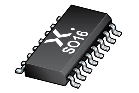
| 74LV4094D | 1.0 - 3.6 | TTL | ± 6 | 14 | 95 | 8 | low | -40~125 | SO16 |
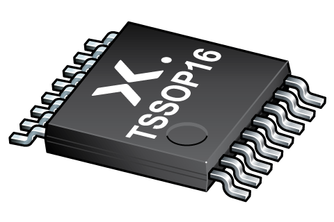
| 74LV4094PW | 1.0 - 3.6 | TTL | ± 6 | 14 | 95 | 8 | low | -40~125 | TSSOP16 |
Package
| Type number | Orderable part number, (Ordering code (12NC)) | Status | Marking | Package | Package information | Reflow-/Wave soldering | Packing |
|---|---|---|---|---|---|---|---|
| 74LV4094D | 74LV4094D,118 (935088040118) |
Active | 74LV4094D |
SO16 (SOT109-1) |
SOT109-1 |
SO-SOJ-REFLOW
SO-SOJ-WAVE WAVE_BG-BD-1 |
SOT109-1_118 |
| 74LV4094PW | 74LV4094PW,118 (935175020118) |
Active | LV4094 |
TSSOP16 (SOT403-1) |
SOT403-1 |
SSOP-TSSOP-VSO-WAVE
|
SOT403-1_118 |
All type numbers in the table below are discontinued.
| Type number | Orderable part number, (Ordering code (12NC)) | Status | Marking | Package | Package information | Reflow-/Wave soldering | Packing |
|---|---|---|---|---|---|---|---|
| 74LV4094DB | 74LV4094DB,112 (935166090112) |
Obsolete | no package information | ||||
| 74LV4094DB,118 (935166090118) |
Obsolete | ||||||
| 74LV4094PW | 74LV4094PW,112 (935175020112) |
Withdrawn / End-of-life | LV4094 |
TSSOP16 (SOT403-1) |
SOT403-1 |
SSOP-TSSOP-VSO-WAVE
|
Not available |
Environmental information
| Type number | Orderable part number | Chemical content | RoHS | RHF-indicator |
|---|---|---|---|---|
| 74LV4094D | 74LV4094D,118 | 74LV4094D |
|
|
| 74LV4094PW | 74LV4094PW,118 | 74LV4094PW |
|
|
All type numbers in the table below are discontinued.
| Type number | Orderable part number | Chemical content | RoHS | RHF-indicator |
|---|---|---|---|---|
| 74LV4094DB | 74LV4094DB,112 | 74LV4094DB |
|
|
| 74LV4094DB | 74LV4094DB,118 | 74LV4094DB |
|
|
| 74LV4094PW | 74LV4094PW,112 | 74LV4094PW |
|
|
Documentation (14)
| File name | Title | Type | Date |
|---|---|---|---|
| 74LV4094 | 8-stage shift-and-store bus register | Data sheet | 2024-05-28 |
| 001aaf118 | Block diagram: 74LV4094D, 74LV4094DB, 74LV4094N, 74LV4094PW | Block diagram | 2009-11-04 |
| SOT109-1 | 3D model for products with SOT109-1 package | Design support | 2020-01-22 |
| SOT403-1 | 3D model for products with SOT403-1 package | Design support | 2020-01-22 |
| Nexperia_package_poster | Nexperia package poster | Leaflet | 2020-05-15 |
| SO16_SOT109-1_mk | plastic, small outline package; 16 leads; 1.27 mm pitch; 9.9 mm x 3.9 mm x 1.35 mm body | Marcom graphics | 2017-01-28 |
| TSSOP16_SOT403-1_mk | plastic, thin shrink small outline package; 16 leads; 0.65 mm pitch; 5 mm x 4.4 mm x 1.1 mm body | Marcom graphics | 2017-01-28 |
| SOT109-1 | plastic, small outline package; 16 leads; 1.27 mm pitch; 9.9 mm x 3.9 mm x 1.75 mm body | Package information | 2023-11-07 |
| SOT403-1 | plastic, thin shrink small outline package; 16 leads; 5 mm x 4.4 mm x 1.2 mm body | Package information | 2023-11-08 |
| SO-SOJ-REFLOW | Footprint for reflow soldering | Reflow soldering | 2009-10-08 |
| Nexperia_Selection_guide_2023 | Nexperia Selection Guide 2023 | Selection guide | 2023-05-10 |
| SO-SOJ-WAVE | Footprint for wave soldering | Wave soldering | 2009-10-08 |
| WAVE_BG-BD-1 | Wave soldering profile | Wave soldering | 2021-09-08 |
| SSOP-TSSOP-VSO-WAVE | Footprint for wave soldering | Wave soldering | 2009-10-08 |
Support
If you are in need of design/technical support, let us know and fill in the answer form we'll get back to you shortly.
Ordering, pricing & availability
Sample
As a Nexperia customer you can order samples via our sales organization.
If you do not have a direct account with Nexperia our network of global and regional distributors is available and equipped to support you with Nexperia samples. Check out the list of official distributors.