74AVCH1T45-Q100
Dual-supply voltage level translator/transceiver; 3-state
The 74AVCH1T45-Q100 is a single bit, dual supply transceiver that enables bidirectional level translation. The 74AVCH1T45 has active bus hold circuitry which is provided to hold unused or floating data inputs at a valid logic level. The device is fully specified for partial power-down applications using IOFF. The IOFF circuitry disables the output, preventing potentially damaging backflow current through the device when it is powered down.
This product has been qualified to the Automotive Electronics Council (AEC) standard Q100 (Grade 1) and is suitable for use in automotive applications.
Features and benefits
Automotive product qualification in accordance with AEC-Q100 (Grade 1)
Specified from -40 °C to +85 °C and from -40 °C to +125 °C
Wide supply voltage range from 0.8 V to 3.6 V
High noise immunity
CMOS low power dissipation
Overvoltage tolerant inputs to 3.6 V
Dynamically controlled outpus
Complies with JEDEC standards:
JESD8-12 (0.8 V to 1.3 V)
JESD8-11 (0.9 V to 1.65 V)
JESD8-7 (1.2 V to 1.95 V)
JESD8-5 (1.8 V to 2.7 V)
JESD8-B (2.7 V to 3.6 V)
Maximum data rates:
500 Mbit/s (1.8 V to 3.3 V translation)
320 Mbit/s (< 1.8 V to 3.3 V translation)
320 Mbit/s (translate to 2.5 V or 1.8 V)
280 Mbit/s (translate to 1.5 V)
240 Mbit/s (translate to 1.2 V)
Suspend mode
Bus hold on data inputs
Latch-up performance exceeds 100 mA per JESD 78 Class II
Low noise overshoot and undershoot < 10 % of VCC
IOFF circuitry provides partial Power-down mode operation
ESD protection:
HBM: ANSI/ESDA/JEDEC JS-001 class 3B exceeds 8000 V
CDM: ANSI/ESDA/JEDEC JS-002 class C3 exceeds 1000 V
Parametrics
| Type number | VCC(A) (V) | VCC(B) (V) | Logic switching levels | Output drive capability (mA) | tpd (ns) | Nr of bits | Power dissipation considerations | Tamb (°C) | Package name |
|---|---|---|---|---|---|---|---|---|---|
| 74AVCH1T45GW-Q100 | 0.8 - 3.6 | 0.8 - 3.6 | CMOS/LVTTL | ± 12 | 2.1 | 1 | very low | -40~125 | TSSOP6 |
Package
| Type number | Orderable part number, (Ordering code (12NC)) | Status | Marking | Package | Package information | Reflow-/Wave soldering | Packing |
|---|---|---|---|---|---|---|---|
| 74AVCH1T45GW-Q100 | 74AVCH1T45GW-Q100H (935299267125) |
Active | K5 |
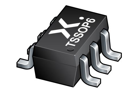
TSSOP6 (SOT363-2) |
SOT363-2 | SOT363-2_125 |
Environmental information
| Type number | Orderable part number | Chemical content | RoHS | RHF-indicator |
|---|---|---|---|---|
| 74AVCH1T45GW-Q100 | 74AVCH1T45GW-Q100H | 74AVCH1T45GW-Q100 |
|
|
Documentation (7)
| File name | Title | Type | Date |
|---|---|---|---|
| 74AVCH1T45_Q100 | Dual-supply voltage level translator/transceiver; 3-state | Data sheet | 2024-07-02 |
| AN10161 | PicoGate Logic footprints | Application note | 2002-10-29 |
| AN90007 | Pin FMEA for AVC family | Application note | 2018-11-30 |
| SOT363-2 | 3D model for products with SOT363-2 package | Design support | 2023-02-02 |
| avch1t45 | 74AVCH1T45 Ibis model | IBIS model | 2014-10-14 |
| SOT363-2 | plastic thin shrink small outline package; 6 leads; body width 1.25 mm | Package information | 2022-11-21 |
| Nexperia_Selection_guide_2023 | Nexperia Selection Guide 2023 | Selection guide | 2023-05-10 |
Support
If you are in need of design/technical support, let us know and fill in the answer form we'll get back to you shortly.
Ordering, pricing & availability
Sample
As a Nexperia customer you can order samples via our sales organization.
If you do not have a direct account with Nexperia our network of global and regional distributors is available and equipped to support you with Nexperia samples. Check out the list of official distributors.