74ALVCH16500
18-bit universal bus transceiver; 3-state
The 74ALVCH16500 is an 18-bit universal transceiver with bus hold inputs and 3-state outputs. Data flow in each direction is controlled by output enable (OEAB and OEBA), latch enable (LEAB and LEBA), and clock (CPAB and CPBA) inputs. For A-to-B data flow, the device operates in the transparent mode when LEAB is HIGH. When LEAB is LOW, the A data is latched if CPAB is held at a HIGH or LOW logic level. If LEAB is LOW, the A-bus data is stored in the latch/flip-flop on the HIGH-to-LOW transition of CPAB. When OEAB is HIGH, the outputs are active. When OEAB is LOW, the outputs are in the high-impedance state.
Data flow for B-to-A is similar to that of A-to-B but uses OEBA, LEBA and CPBA. The output enables are complimentary (OEAB is active HIGH, and OEBA is active LOW). This device is fully specified for partial power down applications using IOFF. The IOFF circuitry disables the output, preventing the potentially damaging backflow current through the device when it is powered down.
Features and benefits
Wide supply voltage range from 1.65 V to 3.6 V
CMOS low power dissipation
MULTIBYTE™ flow-through standard pin-out architecture
Low inductance multiple VCC and GND pins for minimum noise and ground bounce
Direct interface with TTL levels (2.7 V to 3.6 V)
Bus hold on data inputs
Latch-up performance exceeds 100 mA per JESD 78 Class II Level B
Output drive capability 50 Ω transmission lines at 85 °C
Current drive ±24 mA at 3.0 V
Complies with JEDEC standards:
JESD8-7 (1.65 V to 1.95 V)
JESD8-5 (2.3 V to 2.7 V)
JESD8C/JESD36 (2.7 V to 3.6 V)
ESD protection:
HBM: ANSI/ESDA/JEDEC JS-001 class 2 exceeds 2000 V
CDM: ANSI/ESDA/JEDEC JS-002 class C3 exceeds 1000 V
Specified from -40 °C to +85 °C
Parametrics
| Type number | VCC(A) (V) | VCC(B) (V) | Logic switching levels | Output drive capability (mA) | tpd (ns) | Nr of bits | fmax (MHz) | Power dissipation considerations | Tamb (°C) | Package name |
|---|---|---|---|---|---|---|---|---|---|---|
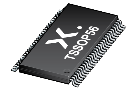
| 74ALVCH16500DGG | n.a. | n.a. | TTL | ± 24 | 2.9 | 18 | 150 | low | -40~85 | TSSOP56 |
Package
| Type number | Orderable part number, (Ordering code (12NC)) | Status | Marking | Package | Package information | Reflow-/Wave soldering | Packing |
|---|---|---|---|---|---|---|---|
| 74ALVCH16500DGG | 74ALVCH16500DGG:11 (935262542118) |
Active | ALVCH16500 |
TSSOP56 (SOT364-1) |
SOT364-1 |
SSOP-TSSOP-VSO-WAVE
|
SOT364-1_118 |
Environmental information
| Type number | Orderable part number | Chemical content | RoHS | RHF-indicator |
|---|---|---|---|---|
| 74ALVCH16500DGG | 74ALVCH16500DGG:11 | 74ALVCH16500DGG |
|
|
Documentation (8)
| File name | Title | Type | Date |
|---|---|---|---|
| 74ALVCH16500 | 18-bit universal bus transceiver; 3-state | Data sheet | 2024-06-28 |
| sw00090 | Block diagram: 74ALVCH16500DGG | Block diagram | 2009-11-03 |
| SOT364-1 | 3D model for products with SOT364-1 package | Design support | 2020-01-22 |
| alvch16500 | alvch16500 IBIS model | IBIS model | 2013-04-08 |
| Nexperia_package_poster | Nexperia package poster | Leaflet | 2020-05-15 |
| SOT364-1 | plastic, thin shrink small outline package; 56 leads; 0.5 mm pitch; 14 mm x 6.1 mm x 1.2 mm body | Package information | 2022-06-23 |
| Nexperia_Selection_guide_2023 | Nexperia Selection Guide 2023 | Selection guide | 2023-05-10 |
| SSOP-TSSOP-VSO-WAVE | Footprint for wave soldering | Wave soldering | 2009-10-08 |
Support
If you are in need of design/technical support, let us know and fill in the answer form we'll get back to you shortly.
Models
| File name | Title | Type | Date |
|---|---|---|---|
| SOT364-1 | 3D model for products with SOT364-1 package | Design support | 2020-01-22 |
| alvch16500 | alvch16500 IBIS model | IBIS model | 2013-04-08 |
Ordering, pricing & availability
Sample
As a Nexperia customer you can order samples via our sales organization.
If you do not have a direct account with Nexperia our network of global and regional distributors is available and equipped to support you with Nexperia samples. Check out the list of official distributors.