
74AVC1T1022
1-to-4 fan-out buffer
The 74AVC1T1022 is a translating 1-to-4 fan-out buffer suitable for use in clock distribution. It has dual supplies (VCC(A) and VCC(B)) for voltage translation. It also has a data input (A), four data outputs (1Yn and 2Yn) and an output enable input (OE). VCC(A) and VCC(B) can be independently supplied at any voltage between 0.8 V and 3.6 V. It makes the device suitable for low voltage translation between any of the following voltages: 0.8 V, 1.2 V, 1.5 V, 1.8 V, 2.5 V and 3.3 V. The levels of A, OE and 1Yn are referenced to VCC(A), outputs 2Yn are referenced to VCC(B). This supply configuration ensures that two of the fanned out signals can be used in level shifting. A HIGH on OE causes all outputs to be pulled LOW via pull-down resistors, a LOW on OE disconnects the pull-down resistors and enables all outputs.
Schmitt trigger action at all inputs makes the circuit tolerant for slower input rise and fall time.
The IOFF circuitry disables the output, preventing any damaging backflow current through the device when it is powered down.
Features and benefits
Wide supply voltage range:
VCC(A): 0.8 V to 3.6 V
VCC(B): 0.8 V to 3.6 V
Complies with JEDEC standards:
JESD8-12 (0.8 V to 1.3 V)
JESD8-11 (0.9 V to 1.65 V)
JESD8-7 (1.2 V to 1.95 V)
JESD8-5 (1.8 V to 2.7 V)
JESD8-B (2.7 V to 3.6 V)
Maximum data rates:
380 Mbit/s (≥ 1.8 V to 3.3 V translation)
200 Mbit/s (≥ 1.1 V to 3.3 V translation)
200 Mbit/s (≥ 1.1 V to 2.5 V translation)
200 Mbit/s (≥ 1.1 V to 1.8 V translation)
150 Mbit/s (≥ 1.1 V to 1.5 V translation)
100 Mbit/s (≥ 1.1 V to 1.2 V translation)
Latch-up performance exceeds 100 mA per JESD 78 Class II
Inputs accept voltages up to 3.6 V
ESD protection:
HBM: ANSI/ESDA/JEDEC JS-001 class 3B exceeds 8000 V
CDM: ANSI/ESDA/JEDEC JS-002 class C3 exceeds 1000 V
Specified from -40 °C to +85 °C and -40 °C to +125 °C
Parametrics
| Type number | VCC(A) (V) | VCC(B) (V) | Logic switching levels | Output drive capability (mA) | tpd (ns) | Nr of bits | Power dissipation considerations | Tamb (°C) | Package name |
|---|---|---|---|---|---|---|---|---|---|
| 74AVC1T1022DP | 0.8 - 3.6 | 0.8 - 3.6 | CMOS/LVTTL | ± 12 | 4.0 | 1 | very low | -40~125 | TSSOP10 |
| 74AVC1T1022GU | 0.8 - 3.6 | 0.8 - 3.6 | CMOS/LVTTL | ± 12 | 4.0 | 1 | very low | -40~125 | XQFN10 |
Package
| Type number | Orderable part number, (Ordering code (12NC)) | Status | Marking | Package | Package information | Reflow-/Wave soldering | Packing |
|---|---|---|---|---|---|---|---|
| 74AVC1T1022DP | 74AVC1T1022DPJ (935305831118) |
Active | B2 |
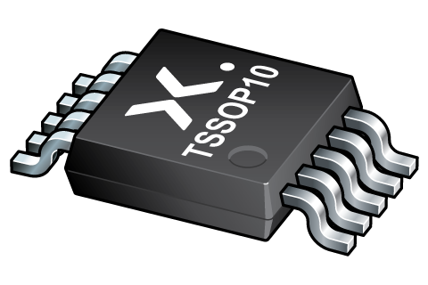
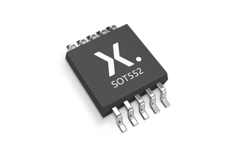
TSSOP10 (SOT552-1) |
SOT552-1 |
SSOP-TSSOP-VSO-WAVE
|
SOT552-1_118 |
| 74AVC1T1022GU | 74AVC1T1022GUX (935305832115) |
Active | B2 |
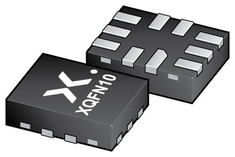
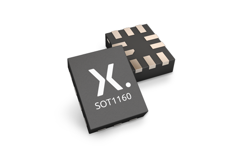
XQFN10 (SOT1160-1) |
SOT1160-1 | SOT1160-1_115 |
Environmental information
| Type number | Orderable part number | Chemical content | RoHS | RHF-indicator |
|---|---|---|---|---|
| 74AVC1T1022DP | 74AVC1T1022DPJ | 74AVC1T1022DP |
|
|
| 74AVC1T1022GU | 74AVC1T1022GUX | 74AVC1T1022GU |
|
|
Documentation (14)
| File name | Title | Type | Date |
|---|---|---|---|
| 74AVC1T1022 | 1-to-4 fan-out buffer | Data sheet | 2024-06-25 |
| Nexperia_document_guide_Logic_translators | Nexperia Logic Translators | Brochure | 2021-04-12 |
| Nexperia_document_guide_MiniLogic_PicoGate_201901 | PicoGate leaded logic portfolio guide | Brochure | 2019-01-07 |
| Nexperia_document_guide_MiniLogic_MicroPak_201808 | MicroPak leadless logic portfolio guide | Brochure | 2018-09-03 |
| SOT552-1 | 3D model for products with SOT552-1 package | Design support | 2020-01-22 |
| SOT1160-1 | 3D model for products with SOT1160-1 package | Design support | 2019-10-03 |
| avc1t1022 | 74AVC1T1022 IBIS model | IBIS model | 2015-10-26 |
| Nexperia_package_poster | Nexperia package poster | Leaflet | 2020-05-15 |
| TSSOP10_SOT552_mk | plastic, thin shrink small outline package; 10 leads; 0.5 mm pitch; 3 mm x 3 mm x 1.1 mm body | Marcom graphics | 2017-01-28 |
| XQFN10_SOT1160-1_mk | plastic, extremely thin quad flat package; no leads; 10 terminals; 0.4 mm pitch; 1.4 mm x 1.8 mm x 0.5 mm body | Marcom graphics | 2017-01-28 |
| SOT552-1 | plastic, thin shrink small outline package; 10 leads; 0.5 mm pitch; 3 mm x 3 mm x 1.1 mm body | Package information | 2022-06-07 |
| SOT1160-1 | plastic, leadless extremely thin quad flat package; 10 terminals; 0.4 mm pitch; 1.4 mm x 1.8 mm x 0.5 mm body | Package information | 2022-06-07 |
| Nexperia_Selection_guide_2023 | Nexperia Selection Guide 2023 | Selection guide | 2023-05-10 |
| SSOP-TSSOP-VSO-WAVE | Footprint for wave soldering | Wave soldering | 2009-10-08 |
Support
If you are in need of design/technical support, let us know and fill in the answer form we'll get back to you shortly.
Ordering, pricing & availability
Sample
As a Nexperia customer you can order samples via our sales organization.
If you do not have a direct account with Nexperia our network of global and regional distributors is available and equipped to support you with Nexperia samples. Check out the list of official distributors.