
74LVC8T595
Dual supply 8-bit serial-in/serial-out or parallel-out shift register; 3-state
The 74LVC8T595 is an 8-bit serial-in/serial or parallel-out shift register with a storage register and 3-state outputs. Both the shift and storage register have separate clocks. Data is shifted on the positive-going transitions of the SHCP input. The data in the shift register is transferred to the storage register on a positive-going transition of the STCP input. If both clocks are connected together, the shift register is always one clock pulse ahead of the storage register.
VCC(A) and VCC(B) can be supplied at any voltage between 1.1 V and 5.5 V making the device suitable for translating between any of the voltage nodes (1.2 V, 1.5 V, 1.8 V, 2.5 V, 3.3 V and 5.0 V). Pins MR, SHCP, STCP, OE, DS and Q7S are referenced to VCC(A) and pins Qn are referenced to VCC(B).
The device is fully specified for partial power-down applications using IOFF. The IOFF circuitry disables the output, preventing any damaging backflow current through the device when it is powered down. In suspend mode when VCC(A) is at GND level, the Qn outputs are in the high-impedance OFF-state.
Features and benefits
Wide supply voltage range:
VCC(A): 1.1 V to 5.5 V
VCC(B): 1.1 V to 5.5 V
High noise immunity
Suspend mode
Latch-up performance exceeds 100 mA per JESD 78 Class II
±24 mA output drive (VCC(A) = VCC(B) = 3.0 V)
Inputs accept voltages up to 5.5 V
IOFF circuitry provides partial Power-down mode operation
Complies with JEDEC standards:
JESD8-12A (1.1 V to 1.3 V)
JESD8-11A (1.4 V to 1.6 V)
JESD8-7 (1.65 V to 1.95 V)
JESD8-5 (2.3 V to 2.7 V)
JESD8C (3.0 V to 3.6 V)
JESD12-6 (4.5 V to 5.5 V)
ESD protection:
HBM: ANSI/ESDA/JEDEC JS-001 class 3A exceeds 4000 V
CDM: ANSI/ESDA/JEDEC JS-002 class C3 exceeds 1000 V
Specified from -40 °C to +85 °C and -40 °C to +125 °C
Parametrics
| Type number | VCC(A) (V) | VCC(B) (V) | Logic switching levels | Output drive capability (mA) | tpd (ns) | Nr of bits | Power dissipation considerations | Tamb (°C) | Package name |
|---|---|---|---|---|---|---|---|---|---|
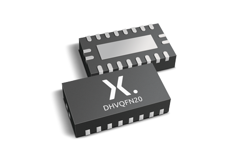
| 74LVC8T595BQ | 1.1 - 5.5 | 1.1 - 5.5 | CMOS/LVTTL | ± 24 | 4.1 | 8 | low | -40~125 | DHVQFN20 |
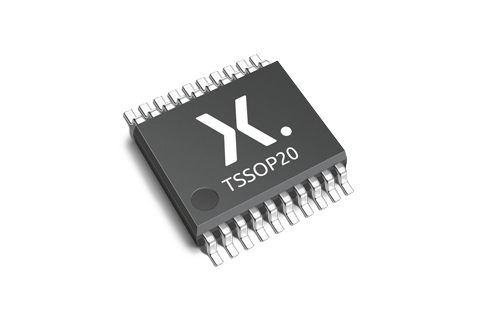
| 74LVC8T595PW | 1.1 - 5.5 | 1.1 - 5.5 | CMOS/LVTTL | ± 24 | 4.1 | 8 | low | -40~125 | TSSOP20 |
Package
| Type number | Orderable part number, (Ordering code (12NC)) | Status | Marking | Package | Package information | Reflow-/Wave soldering | Packing |
|---|---|---|---|---|---|---|---|
| 74LVC8T595BQ | 74LVC8T595BQX (935309143115) |
Active | LVC8T595 |
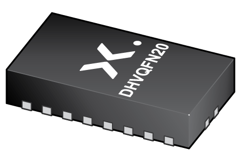
DHVQFN20 (SOT764-1) |
SOT764-1 | SOT764-1_115 | |
| 74LVC8T595PW | 74LVC8T595PWJ (935309144118) |
Active | VC8T595 |
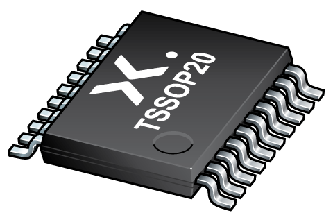
TSSOP20 (SOT360-1) |
SOT360-1 |
SSOP-TSSOP-VSO-WAVE
|
SOT360-1_118 |
Environmental information
| Type number | Orderable part number | Chemical content | RoHS | RHF-indicator |
|---|---|---|---|---|
| 74LVC8T595BQ | 74LVC8T595BQX | 74LVC8T595BQ |
|
|
| 74LVC8T595PW | 74LVC8T595PWJ | 74LVC8T595PW |
|
|
Documentation (12)
| File name | Title | Type | Date |
|---|---|---|---|
| 74LVC8T595 | Dual supply 8-bit serial-in/serial-out or parallel-out shift register; 3-state | Data sheet | 2023-08-29 |
| Nexperia_document_guide_Logic_translators | Nexperia Logic Translators | Brochure | 2021-04-12 |
| SOT764-1 | 3D model for products with SOT764-1 package | Design support | 2019-10-03 |
| SOT360-1 | 3D model for products with SOT360-1 package | Design support | 2020-01-22 |
| Nexperia_document_leaflet_Logic_74LVC8T595_201711 | Voltage-translating Shift Register for Modular Designs | Leaflet | 2017-11-29 |
| Nexperia_package_poster | Nexperia package poster | Leaflet | 2020-05-15 |
| DHVQFN20_SOT764-1_mk | plastic, dual in-line compatible thermal enhanced very thin quad flat package; 20 terminals; 0.5 mm pitch; 2.5 mm x 4.5 mm x 0.85 mm body | Marcom graphics | 2017-01-28 |
| TSSOP20_SOT360-1_mk | plastic, thin shrink small outline package; 20 leads; 0.65 mm pitch; 6.5 mm x 4.4 mm x 1.1 mm body | Marcom graphics | 2017-01-28 |
| SOT764-1 | plastic, leadless dual in-line compatible thermal enhanced very thin quad flat package; 20 terminals; 0.5 mm pitch; 4.5 mm x 2.5 mm x 1 mm body | Package information | 2022-06-21 |
| SOT360-1 | plastic, thin shrink small outline package; 20 leads; 0.65 mm pitch; 6.5 mm x 4.4 mm x 1.1 mm body | Package information | 2022-06-21 |
| Nexperia_Selection_guide_2023 | Nexperia Selection Guide 2023 | Selection guide | 2023-05-10 |
| SSOP-TSSOP-VSO-WAVE | Footprint for wave soldering | Wave soldering | 2009-10-08 |
Support
If you are in need of design/technical support, let us know and fill in the answer form we'll get back to you shortly.
Ordering, pricing & availability
Sample
As a Nexperia customer you can order samples via our sales organization.
If you do not have a direct account with Nexperia our network of global and regional distributors is available and equipped to support you with Nexperia samples. Check out the list of official distributors.