
PESDxUSB3B
ESD protection for differential data lines
ElectroStatic Discharge (ESD) protection for one, two and three differential channels.
The devices are footprint compatible to PCMFxUSB3B/C common mode filters with ESD protection.
Diodes provide protection to downstream components from ESD voltages up to ±20 kV on each signal line.
Type Number | Number of channels | Package name |
|---|---|---|
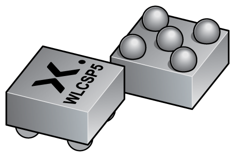
PESD1USB3B/C | 1 | WLCSP5 |
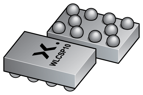
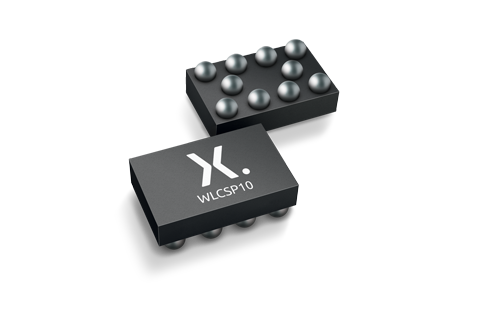
PESD2USB3B/C | 2 | WLCSP10 |
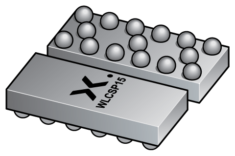
PESD3USB3B/C | 3 | WLCSP15 |
Features and benefits
Allows switching between PCMFxUSB3B/C common mode filters with ESD protection and PESDxUSB3B/C ESD protection in the same footprint
TrEOS protection process for very high system-level ESD robustness: superior protection of sensitive Systems on Chips (SoCs)
ESD protection for one, two and three differential channels up to ±20 kV contact discharge according to IEC 61000-4-2
Industry-standard WLCSP5, 10 and 15 packages for smallest footprint
- Bidirectional for audio line option
Applications
Smartphone, cellular and cordless phone
USB3.2, USB2.0, HDMI2.0, HDMI1.4
General-purpose downstream ESD protection for differential data lines
Tablet PC and Mobile Internet Device (MID)
MIPI D-PHY as used in Camera Serial Interface (CSI) and Display Serial Interface (DSI)
Parametrics
| Type number | Package version | Package name | Size (mm) | Configuration | Nr of lines | VRWM (V) (V) | Cd [typ] (pF) | IPPM [max] (A) | VESD (kV) (kV) |
|---|---|---|---|---|---|---|---|---|---|
| PESD1USB3B | WLCSP5_2-1-2 | WLCSP5 | 0.77 x 1.17 x 0.57 | Bidirectional | 2 | 4 | 0.29 | 9.5 | 20 |
| PESD2USB3B | WLCSP10_4-2-4 | WLCSP10 | 1.57 x 1.17 x 0.57 | Bidirectional | 4 | 4 | 0.29 | 9.5 | 20 |
| PESD3USB3B | WLCSP15_6-3-6 | WLCSP15 | 2.37 x 1.17 x 0.57 | Bidirectional | 6 | 4 | 0.29 | 9.5 | 20 |
Package
| Type number | Orderable part number, (Ordering code (12NC)) | Status | Marking | Package | Package information | Reflow-/Wave soldering | Packing |
|---|---|---|---|---|---|---|---|
| PESD1USB3B | PESD1USB3B/CZ (934660293087) |
Active |
WLCSP5 (WLCSP5_2-1-2) |
WLCSP5_2-1-2 | Not available | ||
| PESD2USB3B | PESD2USB3B/CZ (934660294087) |
Active |
WLCSP10 (WLCSP10_4-2-4) |
WLCSP10_4-2-4 | WLCSP10_PCMF_PESD2USB3X_PCMF2HDMI2X_087 | ||
| PESD3USB3B | PESD3USB3B/CZ (934660295087) |
Active |
WLCSP15 (WLCSP15_6-3-6) |
WLCSP15_6-3-6 | WLCSP15_PCMF_PESD3USB3X_PCMF3HDMI2X_087 |
All type numbers in the table below are discontinued.
| Type number | Orderable part number, (Ordering code (12NC)) | Status | Marking | Package | Package information | Reflow-/Wave soldering | Packing |
|---|---|---|---|---|---|---|---|
| PESD1USB3B | PESD1USB3B/CX (934660293115) |
Withdrawn / End-of-life |
WLCSP5 (WLCSP5_2-1-2) |
WLCSP5_2-1-2 | Not available |
Environmental information
| Type number | Orderable part number | Chemical content | RoHS | RHF-indicator |
|---|---|---|---|---|
| PESD1USB3B | PESD1USB3B/CZ | PESD1USB3B |
|
|
| PESD2USB3B | PESD2USB3B/CZ | PESD2USB3B |
|
|
| PESD3USB3B | PESD3USB3B/CZ | PESD3USB3B |
|
|
All type numbers in the table below are discontinued.
| Type number | Orderable part number | Chemical content | RoHS | RHF-indicator |
|---|---|---|---|---|
| PESD1USB3B | PESD1USB3B/CX | PESD1USB3B |
|
|
Documentation (10)
| File name | Title | Type | Date |
|---|---|---|---|
| PESDXUSB3B_C_SER | ESD protection for differential data lines | Data sheet | 2019-01-29 |
| WLCSP5_2-1-2 | 3D model for products with WLCSP5_2-1-2 package | Design support | 2023-03-13 |
| WLCSP10_4-2-4 | 3D model for products with WLCSP10_4-2-4 package | Design support | 2023-03-13 |
| WLCSP15_6-3-6 | 3D model for products with WLCSP15_6-3-6 package | Design support | 2023-03-13 |
| Nexperia_package_poster | Nexperia package poster | Leaflet | 2020-05-15 |
| WLCSP5_2-1-2_mk | wafer level chip-size package; 5 bumps (2-1-2) | Marcom graphics | 2017-01-28 |
| WLCSP10_4-2-4_mk | wafer level chip-size package; 10 bumps (4-2-4) | Marcom graphics | 2017-01-28 |
| WLCSP5_2-1-2 | wafer level chip-size package; 5 bumps (2-1-2); 0.4 mm pitch; 0.77 x 1.17 x 0.57 mm body | Package information | 2020-04-21 |
| WLCSP10_4-2-4 | wafer level chip-size package; 10 bumps (4-2-4); 0.4 mm pitch; 1.57 x 1.17 x 0.57 mm body | Package information | 2020-04-21 |
| WLCSP15_6-3-6 | wafer level chip-size package; 15 bumps (6-3-6); 0.4 mm pitch; 2.37 x 1.17 x 0.57 mm body | Package information | 2020-04-21 |
Support
If you are in need of design/technical support, let us know and fill in the answer form we'll get back to you shortly.
Models
| File name | Title | Type | Date |
|---|---|---|---|
| WLCSP5_2-1-2 | 3D model for products with WLCSP5_2-1-2 package | Design support | 2023-03-13 |
| WLCSP10_4-2-4 | 3D model for products with WLCSP10_4-2-4 package | Design support | 2023-03-13 |
| WLCSP15_6-3-6 | 3D model for products with WLCSP15_6-3-6 package | Design support | 2023-03-13 |
Ordering, pricing & availability
Sample
As a Nexperia customer you can order samples via our sales organization.
If you do not have a direct account with Nexperia our network of global and regional distributors is available and equipped to support you with Nexperia samples. Check out the list of official distributors.