
PESDxUSB3S
ESD protection for differential data lines
The devices are ElectroStatic Discharge (ESD) protection devices for one, two or three differential channels.
The PESDxUSB3S is footprint compatible to PCMFxUSB3S.
The devices provide protection to downstream components from ESD voltages up to ±15 kV on each signal line.
Type number | Number of channels | Package Name |
|---|---|---|
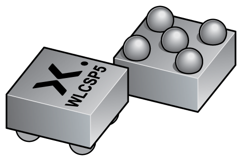
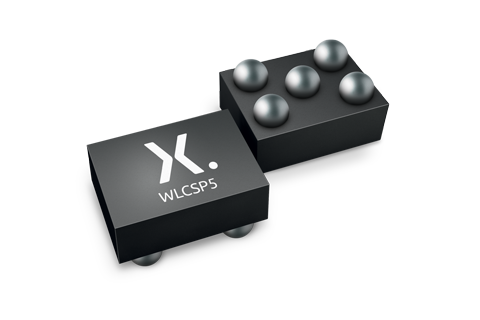
PESD1USB3S | 1 | WLCSP5 |
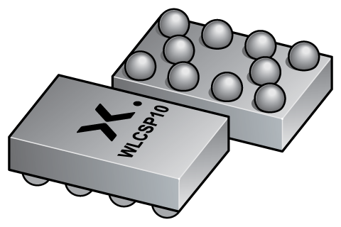
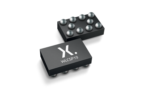
PESD2USB3S | 2 | WLCSP10 |
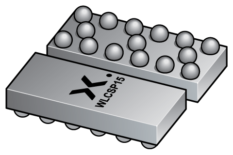
PESD3USB3S | 3 | WLCSP15 |
Features and benefits
Allows replacement between PCMFxUSB3S common-mode filters with ESD protection and PESDxUSB3S ESD protection in the same footprint
TrEOS protection process for very high system-level ESD robustness: superior protection of sensitive SoCs
ESD protection for one, two and three differential channels up to ±15 kV contact discharge according to IEC 61000-4-2
Industry-standard WLCSP5, 10 and 15 packages for smallest footprint
Applications
Smartphone, cellular and cordless phone
USB3.1, USB2.0, HDMI2.0, HDMI1.4
General-purpose downstream ESD protection
Tablet PC and Mobile Internet Device (MID)
MIPI D-PHY as used in Camera Serial Interface (CSI) and Display Serial Interface (DSI)
Parametrics
| Type number | Package version | Package name | Size (mm) | Configuration | Nr of lines | VRWM (V) (V) | Cd [typ] (pF) | IPPM [max] (A) | VESD (kV) (kV) |
|---|---|---|---|---|---|---|---|---|---|
| PESD1USB3S | WLCSP5_2-1-2 | WLCSP5 | 0.77 x 1.17 x 0.57 | Unidirectional | 2 | 5 | 0.45 | 8 | 15 |
| PESD2USB3S | WLCSP10_4-2-4 | WLCSP10 | 1.57 x 1.17 x 0.57 | Unidirectional | 4 | - | 0.45 | 8 | 15 |
| PESD3USB3S | WLCSP15_6-3-6 | WLCSP15 | 2.37 x 1.17 x 0.57 | Unidirectional | 6 | 5 | 0.45 | 8 | 15 |
Package
| Type number | Orderable part number, (Ordering code (12NC)) | Status | Marking | Package | Package information | Reflow-/Wave soldering | Packing |
|---|---|---|---|---|---|---|---|
| PESD1USB3S | PESD1USB3S/CZ (934660289087) |
Active |
WLCSP5 (WLCSP5_2-1-2) |
WLCSP5_2-1-2 | Not available | ||
| PESD1USB3SZ (934069683087) |
Active | Not available | |||||
| PESD2USB3S | PESD2USB3S/CZ (934660291087) |
Active |
WLCSP10 (WLCSP10_4-2-4) |
WLCSP10_4-2-4 | WLCSP10_PCMF_PESD2USB3X_PCMF2HDMI2X_087 | ||
| PESD2USB3SZ (934069684087) |
Active | WLCSP10_PCMF_PESD2USB3X_PCMF2HDMI2X_087 | |||||
| PESD3USB3S | PESD3USB3S/CZ (934660292087) |
Active |
WLCSP15 (WLCSP15_6-3-6) |
WLCSP15_6-3-6 | WLCSP15_PCMF_PESD3USB3X_PCMF3HDMI2X_087 | ||
| PESD3USB3SZ (934069685087) |
Active | WLCSP15_PCMF_PESD3USB3X_PCMF3HDMI2X_087 |
All type numbers in the table below are discontinued.
| Type number | Orderable part number, (Ordering code (12NC)) | Status | Marking | Package | Package information | Reflow-/Wave soldering | Packing |
|---|---|---|---|---|---|---|---|
| PESD3USB3S | PESD3USB3S/CX (934660292115) |
Withdrawn / End-of-life |
WLCSP15 (WLCSP15_6-3-6) |
WLCSP15_6-3-6 | Not available |
Environmental information
| Type number | Orderable part number | Chemical content | RoHS | RHF-indicator |
|---|---|---|---|---|
| PESD1USB3S | PESD1USB3S/CZ | PESD1USB3S |
|
|
| PESD1USB3S | PESD1USB3SZ | PESD1USB3S |
|
|
| PESD2USB3S | PESD2USB3S/CZ | PESD2USB3S |
|
|
| PESD2USB3S | PESD2USB3SZ | PESD2USB3S |
|
|
| PESD3USB3S | PESD3USB3S/CZ | PESD3USB3S |
|
|
| PESD3USB3S | PESD3USB3SZ | PESD3USB3S |
|
|
All type numbers in the table below are discontinued.
| Type number | Orderable part number | Chemical content | RoHS | RHF-indicator |
|---|---|---|---|---|
| PESD3USB3S | PESD3USB3S/CX | PESD3USB3S |
|
|
Documentation (10)
| File name | Title | Type | Date |
|---|---|---|---|
| PESDXUSB3S_SER | ESD protection for differential data lines | Data sheet | 2019-01-30 |
| WLCSP5_2-1-2 | 3D model for products with WLCSP5_2-1-2 package | Design support | 2023-03-13 |
| WLCSP10_4-2-4 | 3D model for products with WLCSP10_4-2-4 package | Design support | 2023-03-13 |
| WLCSP15_6-3-6 | 3D model for products with WLCSP15_6-3-6 package | Design support | 2023-03-13 |
| Nexperia_package_poster | Nexperia package poster | Leaflet | 2020-05-15 |
| WLCSP5_2-1-2_mk | wafer level chip-size package; 5 bumps (2-1-2) | Marcom graphics | 2017-01-28 |
| WLCSP10_4-2-4_mk | wafer level chip-size package; 10 bumps (4-2-4) | Marcom graphics | 2017-01-28 |
| WLCSP5_2-1-2 | wafer level chip-size package; 5 bumps (2-1-2); 0.4 mm pitch; 0.77 x 1.17 x 0.57 mm body | Package information | 2020-04-21 |
| WLCSP10_4-2-4 | wafer level chip-size package; 10 bumps (4-2-4); 0.4 mm pitch; 1.57 x 1.17 x 0.57 mm body | Package information | 2020-04-21 |
| WLCSP15_6-3-6 | wafer level chip-size package; 15 bumps (6-3-6); 0.4 mm pitch; 2.37 x 1.17 x 0.57 mm body | Package information | 2020-04-21 |
Support
If you are in need of design/technical support, let us know and fill in the answer form we'll get back to you shortly.
Models
| File name | Title | Type | Date |
|---|---|---|---|
| WLCSP5_2-1-2 | 3D model for products with WLCSP5_2-1-2 package | Design support | 2023-03-13 |
| WLCSP10_4-2-4 | 3D model for products with WLCSP10_4-2-4 package | Design support | 2023-03-13 |
| WLCSP15_6-3-6 | 3D model for products with WLCSP15_6-3-6 package | Design support | 2023-03-13 |
Ordering, pricing & availability
Sample
As a Nexperia customer you can order samples via our sales organization.
If you do not have a direct account with Nexperia our network of global and regional distributors is available and equipped to support you with Nexperia samples. Check out the list of official distributors.